Overview As a dual RF power detector, MAX2016 can measure the gain measurement of RF circuits or complex superheterodyne transceiver arrays. A key feature of the device is the inclusion of a comparator that can calculate the difference between the two power levels. That is, a simple gain calculation can be easily achieved through this circuit: gain = POUTPUT-PINPUT = POUTA-POUTB = POUTD. However, it is necessary to ensure that the measurement accuracy requirements are met.
Depending on the application, a calibration may be required to eliminate line and coupling losses and differences between devices. The following summarizes several basic calibration methods for RF gain measurement and provides two common examples. The first example describes the gain measurement of a superheterodyne transceiver in detail. The second example shows how to use a calibrated MAX2016 to replace a low-speed and expensive power meter in a factory automatic test equipment (ATE). In Automatic Test Equipment (ATE), we compared the measurement accuracy with and without calibration. Both examples illustrate the importance of the calibration process in measuring equipment.
Typical RF Transceiver Gain Measurement Since the MAX2016 power detector can work in the frequency range from DC to 2.5GHz, the device can be easily configured to measure a single gain module (Figure 1a) or the entire superheterodyne transceiver array Gain (Figure 1b).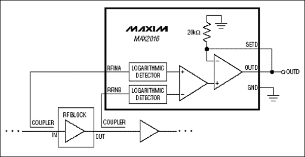
Figure 1a. Gain measurement of a single RF gain module
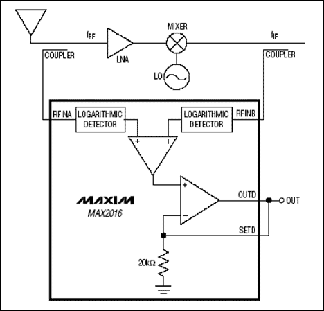
Figure 1b. Gain measurement of a superheterodyne receiver
In the above configuration, the uncertainty of the measurement will affect the accuracy of the gain measurement. The absolute gain measurement will be affected by the difference in the line, the coupler loss, and the difference between the MAX2016 devices. Although MAX2016 integrates two identical logarithmic detectors, small differences in slope and intercept point can cause differential output errors.
A simple way to compensate for these differences is to perform a one-time calibration of the slope and intercept points during factory testing. Figure 2 is a block diagram of the test configuration of the superheterodyne receiver. As shown in the figure, an RF signal with a known power level is fed into the front end of the receiver. Then, an external power detector is used to measure the received power after down conversion. If the down-converted signal is not easy to sample, the on-board high-speed analog-to-digital converter ADC of the transceiver can be used to approximate the received power. Since most receivers use some kind of variable gain amplifier / variable voltage amplifier (VGA / VVA) to improve their dynamic range, the reception can be changed during the test and the subsequent slope measurement and gain-VOUTD response intercept point measurement The gain of the device. By storing the slope and response intercept point in the transceiver's non-volatile memory (NVM), you can map the subsequently measured VOUTD to an absolute gain value. You can also store a matrix of multiple VOUTD and gain values ​​in a non-volatile memory (NVM) to improve accuracy. The interpolation algorithm can be used to calculate the gain corresponding to any measured value of VOUTD. Figure 3 illustrates these two alternatives.
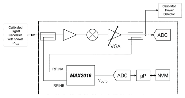
Figure 2. Factory gain calibration equipment-receiver tested
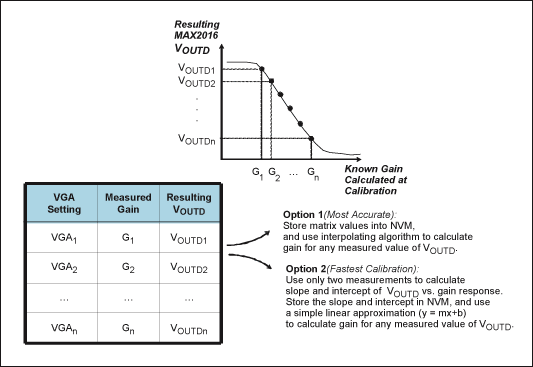
Figure 3. Illustration of gain calibration for a superheterodyne receiver
MAX2016's two internal logarithmic detectors maintain good consistency over the entire temperature range, and there is no need for temperature drift compensation when calculating the absolute gain of the transceiver. If higher accuracy is required, the typical temperature drift can also be measured and stored in non-volatile memory (NVM). By measuring the current operating temperature and interpolating between temperature endpoints, the gain-VOUTD algorithm can add consideration to temperature drift.
Using MAX2016 to replace the two power meters in the automatic test equipment (ATE) As mentioned above, the easiest way to measure the gain of the device under test (DUT) is to measure its input power and output power in dBm, then, The gain can be obtained by subtracting the input power from the output power. In traditional solutions, the use of a power meter to measure broadband power is the only way to obtain accurate measurement results. However, the measurement speed of the power meter is very low, which cannot meet the requirements of rapid measurement of the production environment. The MAX2016 dual-channel log detector has a relatively short response time (~ 100ns), which can achieve fast gain measurement. As mentioned above, coupling the input power of the device under test (DUT) to one port of the MAX2016 and coupling the output power of the device under test (DUT) to the second port of the MAX2016 allows simple gain measurement. The VOUTD pin outputs a DC voltage (VOUTD_MEAS) proportional to the device gain. The gain can be calculated according to the following formula:Gain (dB) = (VOUTD_OFFSET-VOUTD_MEAS) / VOUTD_SLOPE (Equation 1)
Using the uncalibrated VOUTD_OFFSET and VOUTD_SLOPE typical values ​​given in the MAX2016 data sheet, this formula can be simplified to: gain (dB) = (1.0-VOUTD_MEAS) / 0.025. For more information, please refer to the MAX2016 data sheet.
Although this simple expression is useful for calculating gain, we still recommend a calibration process to improve gain measurement accuracy. By performing multiple calibration steps, different degrees of absolute accuracy can be obtained. The following describes a calibration method in detail, this method requires measuring the accurate values ​​of VOUTD_OFFSET and VOUTD_SLOPE. According to different accuracy requirements, users can choose to perform one or two calibrations. This article compares the accuracy obtained by using VOUTD_OFFSET calibration and VOUTD_OFFSET and VOUTD_SLOPE calibration (see below).
In order to obtain a more accurate VOUTD_OFFSET, the universal test device inputs the same power level at the two input ports of MAX2016. The output DC voltage at the VOUTD pin is equal to VOUTD_OFFSET. Connect a calibrated attenuator in series with an input port of MAX2016 to measure VOUTD, and the user can solve the corresponding VOUTD_SLOPE value according to the given VOUTD_OFFSET and attenuator loss. Fig. 4 is a block diagram of a test device. This gain measurement / calibration scheme uses a MAX2016 evaluation board.
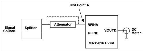
Figure 4. Laboratory evaluation device
This evaluation method uses a fixed power attenuator to calibrate VOUTD_SLOPE. But the results obtained are also applicable to other gain devices. The frequency and precise attenuation are determined by the test requirements of the MAX3654 variable gain amplifier (VGA). The MAX3654 is a CATV transimpedance amplifier with automatic gain control (AGC), and the gain range is 0dB to 20dB. In other applications, different frequencies and attenuators can be selected according to requirements.
Calibrate VOUTD_OFFSET and VOUTD_SLOPE
First use the URV5 RF power meter to measure different attenuators. Subsequently, measurement is performed at point A in FIG. 4 to accurately represent the true attenuation, including cable loss.
Next, measure VOUTD_OFFSET and VOUTD_SLOPE separately at each test frequency.
To measure VOUTD_OFFSET, bypass the attenuator and input the same signal level at the two input ports of MAX2016. In this way, the output DC voltage of the VOUTD pin is the calibration value of OUTD_OFFSET. To measure VOUTD_SLOPE, connect a calibrated 10dB attenuator in series, and measure the output DC voltage of the VOUTD pin again (define this value as VOUTD_MEAS). Given VOUTD_OFFSET and VOUTD_MEAS, and the attenuation of the attenuator is known to be 10dB, VOUTD_SLOPE can be calculated using Equation 1. The attenuation of the attenuator represents the gain of -10dB in Equation 1. Because 10dB is the middle value of the MAX3654 gain range, we chose 10dB attenuation. Table 1 lists the corresponding values ​​of VOUTD_OFFSET and VOUTD_SLOPE. Table 1. Offset and slope calibration| VOUTD_OFFSET (V) | VOUTD_SLOPE (mV / dB) | |
| At 50MHz | 1.044 | 27.8 |
| At 900MHz | 1.043 | 26.3 |
The calibration accuracy comparison uses six independent attenuators (1, 2, 8, 10, 12 and 20dB), and measures VOUTD at each test frequency. In this way, the attenuation values ​​and corresponding accuracy measured in the following three cases can be obtained by calculation: Without calibration, only offset calibration is performed. Offset and slope calibration are performed.
Table 2. The measurement error of MAX2016 uses the typical values ​​in the data sheet (VOUTD_OFFSET = 1.0V, VOUTD_SLOPE = 25mV / dB)
| VOUTD (V) | CALIBRATED ATTENUATION (dB) | MEASURED ATTENUATION (dB) | MEASUREMENT ERROR (dB) |
| 1.022 | 0.9 | 0.9 | 0.0 |
| 0.993 | 2.0 | 0.3 | -1.7 |
| 0.827 | 7.9 | 6.9 | -1.0 |
| 0.763 | 10.1 | 9.5 | -0.6 |
| 0.713 | 11.9 | 11.5 | -0.4 |
| 0.481 | 20.2 | 19.2 | -1.0 |
Table 3. MAX2016 measurement error when operating at 50MHz and only performing offset calibration (the typical value given in the data sheet is VOUTD_SLOPE = 25mV)
| VOUTD (V) | CALIBRATED ATTENUATION (dB) | MEASURED ATTENUATION (dB) | MEASUREMENT ERROR (dB) |
| 1.022 | 0.9 | 0.9 | 0.0 |
| 0.993 | 2.0 | 2.0 | 0.0 |
| 0.827 | 7.9 | 8.7 | 0.8 |
| 0.763 | 10.1 | 11.2 | 1.1 |
| 0.713 | 12.0 | 13.2 | 1.2 |
| 0.481 | 20.2 | 22.5 | 2.3 |
Table 4. Measurement error of MAX2016 after working at 50MHz and performing both offset calibration and slope calibration
| VOUTD (V) | CALIBRATEDB ATTENUATION (dB) | MEASURED ATTENUATION (dB) | MEASUREMENT ERROR (dB) |
| 1.022 | 0.9 | 0.8 | -0.1 |
| 0.993 | 2.0 | 1.9 | -0.1 |
| 0.827 | 7.9 | 7.8 | -0.1 |
| 0.763 | 10.1 | 10.1 | 0.0 |
| 0.713 | 12.0 | 12.0 | 0.0 |
| 0.481 | 20.2 | 20.2 | 0.0 |
Table 5. MAX2016 measurement error when operating at 900MHz and only performing offset calibration (the typical value given in the data sheet is VOUTD_SLOPE = 25mV)
| VOUTD (V) | CALIBRATED ATTENUATION (dB) | MEASURED ATTENUATION (dB) | MEASUREMENT ERROR (dB) |
| 1.021 | 0.9 | 0.9 | 0.0 |
| 0.994 | 2.0 | 2.0 | 0.0 |
| 0.834 | 7.9 | 8.4 | 0.5 |
| 0.774 | 10.1 | 10.8 | 0.7 |
| 0.720 | 12.0 | 12.9 | 0.9 |
| 0.509 | 20.2 | 21.4 | 1.2 |
Table 6. The measurement error of MAX2016 after working at 900MHz and performing both offset calibration and slope calibration
| VOUTD (V) | CALIBRATED ATTENUATION (dB) | MEASURED ATTENUATION (dB) | MEASUREMENT ERROR (dB) |
| 1.021 | 0.9 | 0.9 | 0.0 |
| 0.994 | 2.0 | 1.9 | -0.1 |
| 0.834 | 7.9 | 8.0 | 0.1 |
| 0.774 | 10.1 | 10.1 | 0.0 |
| 0.720 | 12.0 | 12.1 | 0.1 |
| 0.509 | 20.2 | 20.3 | 0.1 |
We can draw the following conclusions by observing the data given above using MAX2016 as the production test for RF detectors.
First, when there is no calibration, the measurement error (Table 2) is large. If devices such as the MAX3654 automatic gain amplifier (VGA) use the uncalibrated MAX2016 to measure gain during production, the test requirements for the automatic gain amplifier (VGA) must be relaxed in consideration of the larger errors it generates. Therefore, the gain index in the data is relaxed accordingly, thus losing the attractiveness to the designer.
Secondly, for attenuators with attenuation values ​​of 0.9dB and 2.0dB, the error can be controlled when only offset calibration is performed (Table 3 and Table 5). This is very useful for measuring a DUT with only one gain value. If the DUT circuit board has been designed and the attenuation at the output of the DUT is equal to the expected typical gain, then the input level at the power detector port is approximately equal. Assuming that the change in the gain index is less than 2dB, the accuracy obtained for the attenuators of 0.9dB and 2.0dB shows that only the offset calibration is required to obtain accurate measurement results. However, as the attenuation value increases, the measurement accuracy will rapidly decrease. Therefore, this method will have problems when measuring VGAs with large gain deviations such as MAX3654.
Tables 4 and 6 show that gains with a wide range of changes in measurement, while calibrating offset and slope, can obtain accurate results. In order to calibrate, the DUT must be able to input the same signal level at the power detection port of the MAX2016, and can switch between calibrated attenuators.
Figure 5 provides an example of a MAX2016 input RF switch. When measuring the gain of the DUT, switch the switch to position A. When performing offset calibration, switch the switch to position B. When performing slope calibration, switch the switch to position C. The attenuation value used when calibrating the slope is equal to the typical value of the DUT gain. Even if an attenuation value (10 dB) that differs greatly from the slope calibration value is used, the resulting error is still small. The data shows that it is correct to assume that the gain-VOUTD curve has minimal nonlinearity, and it is recommended that only slope calibration be used.
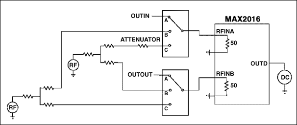
Figure 5. MAX2016RF input calibration switch
LED wall washers are high
power LED lights that are used for decorative lighting and highlight, or wash
walls, of buildings, clubs, hotels, stages, parks, plazas, commercial building
facades, art galleries, etc., with different kind of colors.
The LED wall washer can even change their colors while projecting. The RGB LED
wall washer lights can project various colors and change the color by
programming the LED wall washer the way you want to. LED wall washers can be
used for clubs, stages, parks, plazas, commercial building, art gallery,
landscape, architectural decoration, etc.
Indoor Wall Washer,Led Christmas Wall Washer,Led Light Wall Washer,Led Outdoor Wall Washer
ZHONGSHAN G-LIGHTS LIGHTING CO., LTD. , https://www.glightsled.com