Abstract: A DS4424 adjustable-current DAC is used to adjust the margin of a DC-DC converter's output voltage. This arTIcle describes how to properly select the resistor values ​​of a DC-DC converter's feedback divider network when the DS4424 is employed in the design .
IntroducTIonThe DS4424 adjustable-current DAC is similar to the DS4404 adjustable-current DAC with two major differences. First, the DS4424 has 127 setTIngs each for sink and source mode, while the DS4404 has 31 setTIngs. Second, the DS4424's default I²C address is set to 20h, whereas the DS4404's default I²C address is 90h. Both devices' addresses are determined by the states of the A0 and A1 address pins.
This article focuses on the DS4424, which can be used to adjust the margin of a DC-DC converter's output voltage. The article explains how to properly select resistor values ​​of the DC-DC converter's feedback divider network when the DS4424 is employed in the design .
The Adjustable Power SupplyThe DS4424 contains four I²C adjustable current sources capable of sinking and sourcing current. A typical application for these DACs is margining the output voltage of a DC-DC converter (Figure 1).
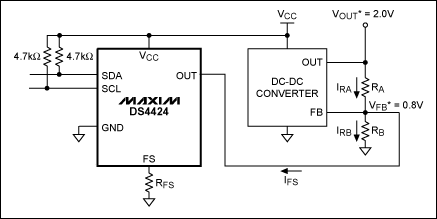
Figure 1. DC-DC converter circuit with adjustable-current DACs used to margin the converter's output voltage. * VOUT and VFB values ​​are determined by the DC-DC converter, and should not be confused with VOUT and VRFS of the DS4424.
The DS4424 sinks and sources from its OUT pins. Valid full-scale current values ​​range from 50µA to 200µA. The value of the full-scale current, IFS, is determined by the size of the resistor connected to the DAC's FS pin of the corresponding OUT pin. The source / sink current generated by the DS4424 is commonly used to adjust the DC-DC converter's feedback voltage-divider.
Determining the Relationship Between VOUT and IFSChoosing the right IFS depends on how much margin is desired on the DC-DC converter's VOUT pin. To determine this margin, we must discover the relationship between VOUT and IFS.
Summing currents into the VFB node, we find that:

Where:

And:

However, since RB and VFB are constant, there is no change in IRB. Thus:

We are looking for the relationship between the margin on VOUT, ΔVOUT, and the selected range of IFS, ΔIFS. Since we know that the change in the IFS current equals the change in the current across RA, we can subtract one set of VOUT and IRA values ​​from the other to determine the relationship between VOUT and IFS.
First, solving Equation 3 to find VOUT, we determine that:

Use Equation 5 to create two equations. For one equation, we choose the maximum margin on VOUT, VOUTMAX, and the maximum IRA current, IRAMAX. For the other equation, we choose the nominal values ​​for VOUT and IRA, VOUTNOM and IRANOM. Subtracting the two equations, we get:
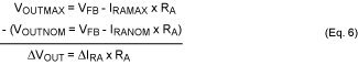
Using Equation 4, Equation 6 translates into the relationship:

Equation 7 shows that the relationship between the margin on VOUT and IFS is determined by the value of the resistor RA.
Calculating the Right Resistor Value for the Margin on VOUTNow that we know the relationship between VOUT and IFS, we can select the correct value of RA and, thus, RB to generate the desired margin on VOUT. Since the full-scale current sink / source range of the DS4424 is 50µA to 200µA, we select 100µA as the IFS current for the DAC. To set this value, choose RFS based on the following equation (also found on page 6 of the DS4424 data sheet):

With VRFS = 0.976V, we solve Equation 8 and find that RFS needs to be 80kΩ (77.47kΩ) to produce a 100µA full-scale current.
With the DS4424 IFS selected, we must determine the size of RA to achieve the desired margin on VOUT. A 2.0V VOUT with a 20% margin requires ± 0.4V of change. Sinking and sourcing the settings of the DS4424 will manage the sign. The change in IFS equals the IFS value of 1mA, and the desired change in VOUT is 0.4V. After substituting for ΔVOUT and ΔIFS in Equation 7, we solve for RA and get RA = 4.0kΩ.
Determining the Relationship Between RA and RBThe feedback network of the circuit in Figure 1 is a voltage-divider with resistors RA and RB. Looking at Figure 1 and assuming IFS = 0A, we can create a simple voltage-divider equation:

We assume that the desired nominal value for VOUT is 2.0V, and that the DC-DC converter has a feedback voltage, VFB, of 0.8V. Substituting the values ​​for VOUT and VFB, the relationship between RA and RB is determined to be:

We use Equation 10 to solve for RB and get RB = 2.67kΩ.
ConclusionThe resistive-feedback-divider network and the current-sinking / sourcing capabilities of the DS4424 DACs control the margin of VOUT on a DC-DC converter. The relationship between the full-scale current, IFS, to the margin on VOUT is determined by the value of the resistor RA. By choosing the correct IFS value for your application, you can determine the correct resistor values ​​for the feedback divider network, and achieve the desired margin on VOUT.
IntroducTIonThe DS4424 adjustable-current DAC is similar to the DS4404 adjustable-current DAC with two major differences. First, the DS4424 has 127 setTIngs each for sink and source mode, while the DS4404 has 31 setTIngs. Second, the DS4424's default I²C address is set to 20h, whereas the DS4404's default I²C address is 90h. Both devices' addresses are determined by the states of the A0 and A1 address pins.
This article focuses on the DS4424, which can be used to adjust the margin of a DC-DC converter's output voltage. The article explains how to properly select resistor values ​​of the DC-DC converter's feedback divider network when the DS4424 is employed in the design .
The Adjustable Power SupplyThe DS4424 contains four I²C adjustable current sources capable of sinking and sourcing current. A typical application for these DACs is margining the output voltage of a DC-DC converter (Figure 1).
Figure 1. DC-DC converter circuit with adjustable-current DACs used to margin the converter's output voltage. * VOUT and VFB values ​​are determined by the DC-DC converter, and should not be confused with VOUT and VRFS of the DS4424.
The DS4424 sinks and sources from its OUT pins. Valid full-scale current values ​​range from 50µA to 200µA. The value of the full-scale current, IFS, is determined by the size of the resistor connected to the DAC's FS pin of the corresponding OUT pin. The source / sink current generated by the DS4424 is commonly used to adjust the DC-DC converter's feedback voltage-divider.
Determining the Relationship Between VOUT and IFSChoosing the right IFS depends on how much margin is desired on the DC-DC converter's VOUT pin. To determine this margin, we must discover the relationship between VOUT and IFS.
Summing currents into the VFB node, we find that:
Where:
And:
However, since RB and VFB are constant, there is no change in IRB. Thus:
We are looking for the relationship between the margin on VOUT, ΔVOUT, and the selected range of IFS, ΔIFS. Since we know that the change in the IFS current equals the change in the current across RA, we can subtract one set of VOUT and IRA values ​​from the other to determine the relationship between VOUT and IFS.
First, solving Equation 3 to find VOUT, we determine that:
Use Equation 5 to create two equations. For one equation, we choose the maximum margin on VOUT, VOUTMAX, and the maximum IRA current, IRAMAX. For the other equation, we choose the nominal values ​​for VOUT and IRA, VOUTNOM and IRANOM. Subtracting the two equations, we get:
Using Equation 4, Equation 6 translates into the relationship:
Equation 7 shows that the relationship between the margin on VOUT and IFS is determined by the value of the resistor RA.
Calculating the Right Resistor Value for the Margin on VOUTNow that we know the relationship between VOUT and IFS, we can select the correct value of RA and, thus, RB to generate the desired margin on VOUT. Since the full-scale current sink / source range of the DS4424 is 50µA to 200µA, we select 100µA as the IFS current for the DAC. To set this value, choose RFS based on the following equation (also found on page 6 of the DS4424 data sheet):
With VRFS = 0.976V, we solve Equation 8 and find that RFS needs to be 80kΩ (77.47kΩ) to produce a 100µA full-scale current.
With the DS4424 IFS selected, we must determine the size of RA to achieve the desired margin on VOUT. A 2.0V VOUT with a 20% margin requires ± 0.4V of change. Sinking and sourcing the settings of the DS4424 will manage the sign. The change in IFS equals the IFS value of 1mA, and the desired change in VOUT is 0.4V. After substituting for ΔVOUT and ΔIFS in Equation 7, we solve for RA and get RA = 4.0kΩ.
Determining the Relationship Between RA and RBThe feedback network of the circuit in Figure 1 is a voltage-divider with resistors RA and RB. Looking at Figure 1 and assuming IFS = 0A, we can create a simple voltage-divider equation:
We assume that the desired nominal value for VOUT is 2.0V, and that the DC-DC converter has a feedback voltage, VFB, of 0.8V. Substituting the values ​​for VOUT and VFB, the relationship between RA and RB is determined to be:
We use Equation 10 to solve for RB and get RB = 2.67kΩ.
ConclusionThe resistive-feedback-divider network and the current-sinking / sourcing capabilities of the DS4424 DACs control the margin of VOUT on a DC-DC converter. The relationship between the full-scale current, IFS, to the margin on VOUT is determined by the value of the resistor RA. By choosing the correct IFS value for your application, you can determine the correct resistor values ​​for the feedback divider network, and achieve the desired margin on VOUT.
Flexible PCB board, PI material with yellow coverlay. 2oz copper on double-side and the surface treatment is ENIG, Total board thickness is only 0.18mm. The characteristic of the Flex board is easy to bend, which is widely used in the instrument.
Our production capacity of flexible PCB is increasing, now we can make flex and Rigid-Flex PCB with high quality, professional services, and fast delivery.
Flexible PCB
Flexible PCB,Professional Flexible PCB,Flexible PCB For Display,Flex PCB Board
Orilind Limited Company , https://www.orilind.com