Introduction Advances in semiconductor technology have greatly increased the number and function of transistors in a chip. This scale of integration was unimaginable a few years ago. Now we realize that without the equally exciting development of IC packaging technology, it is impossible to realize the design of portable electronic products. Driven by the miniaturization of consumer products and the trend of lighter and thinner, manufacturers have developed smaller package types. The smallest package is of course the chip itself. Figure 1 describes the IC's implementation process from wafer to single chip, and Figure 2 is an actual wafer-level package (CSP).
The concept of wafer-level packaging originated in 1990. In the CSP classification defined in 1998, wafer-level CSP is a low-cost choice for a variety of applications, including EEPROM and other small-pin-count devices, as well as ASIC and micro Processor etc. CSP is processed using a process called wafer-level packaging (WLP). The main advantage of WLP is that all assembly and testing are performed on the wafer. As the wafer size increases and the die shrinks, the cost of WLP continues to decrease. As the first company to adopt this technology, Dallas Semiconductor began selling wafer-level packaging products in 1999.
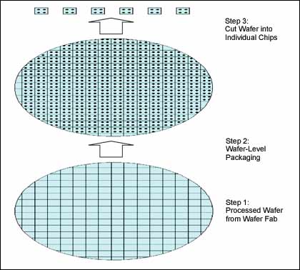
Figure 1. Wafer-level packaging (simplified) finally separates each chip from the processed wafer.
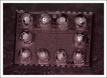
Figure 2. 12 solder ball wafer level package, 3 x 4 solder balls, 2 empty solder ball locations
The naming rules industry still has differences on the naming of WLP. CSP wafer-level technology is very unique, and no bonding is used inside the package. There are also differences in the naming of packaged chips. Common names are: flip chip (STMicroelectronics and Dallas Semiconductor®), CSP, wafer-level packaging, WLCSP, WL-CSP, MicroSMD (NaTIonal Semiconductor), UCSP (Maxim Integrated Products), raised die and MicroCSP (Analog Devices) Wait.
For Maxim® / Dallas Semiconductor, "flip chip" and "wafer level packaging" were originally synonymous with all wafer level packaging. Over the past few years, packaging has been further subdivided. In this document and all Maxim materials, including the company's website, "flip chip" refers to a wafer-level package die (with gaps on the edges) that can have any shape and can be placed anywhere. "Wafer-level package" refers to a wafer-level package die with solder balls on a well-spaced grid. Figure 3 explains these differences. Note that not all grid locations require solder balls.
The flip chip size in Figure 3 reflects the first generation of Dallas Semiconductor's WLP products; wafer-level package sizes come from various vendors, including Maxim. At present, the key dimensions of the new wafer-level packaging products introduced by Maxim and Dallas Semiconductor are listed in Table 1.
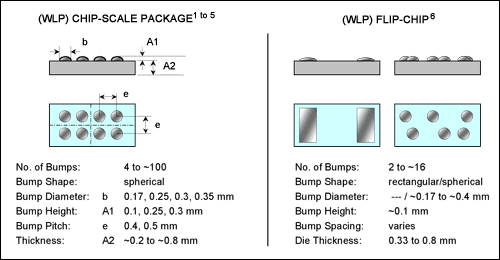
Figure 3. The figure shows typical dimensions and differences between wafer-level packages and flip-chip packages.
Table 1. Nominal dimensions of Maxim and Dallas Semiconductor UCSP (Chip Level Package) 7
| Parameter | Designator | Value |
| No. of Bumps | (---) | 4 to 36 |
| Bump Diameter | b | 0.30, 0.35mm |
| Bump Height | A1 | 0.25, 0.3mm |
| Bump Pitch | e | 0.5mm |
| Die Thickness | A2 | 0.33, 0.38mm |
Wafer-level packaging (WLP) technology Suppliers that provide WLP devices either have their own WLP production lines or outsource packaging processes. Various production processes must be able to meet user requirements to ensure the reliability of the final product. Wafer-Level Packaging Has Arrived 8, The Wafer-Level Packaging EvoluTIon 9, WLCSP Technology DirecTIon 10 and other articles vividly introduce the past and future of WLP. FCI in Phoenix, Arizona, USA, and UniTIve® in North Carolina, USA have established WLP technical standards, and the products are named UltraCSP (FCI) and Xtreme (Unitive). After Amkor acquired Unitive, Amkor provided WLP services for the worldwide semiconductor industry11.
The solder balls connecting the chip and the traces on the circuit / wiring board were originally made of tin-lead eutectic * alloy (Sn63Pb37). In order to reduce harmful substances (RoHS) in electronic products, the semiconductor industry has to use alternative materials, such as lead-free solder balls (Sn96.5Ag3Cu0.5) or high-lead solder balls (Pb95Sn5). Each alloy has its own melting point, therefore, in the component assembly reflow process, the temperature curve is relatively special (maintained at a specific temperature for a period of time).
The purpose of the integrated circuit is to provide all the electronic functions required by the system and can be assembled into a specific package. The bonding pads on the chip are connected to the pins of the common package through wire bonding. The design rules for common packages require the bonding pads to be on the perimeter of the chip. To avoid two designs on the same chip (one for normal packaging and one for CSP), it is necessary to redistribute layers to connect the solder balls and bonding pads.
Determine the feasibility of flip chip / UCSP, meet lead-free requirements Maxim / Dallas Semiconductor only a small number of devices using flip chip or UCSP. The easiest way to identify the package is to use the device on the company's website to quickly browse the web. After a model search, a quick browsing page of data is displayed, which includes a brief description of the device, key features, package selection, URL of the application note, and links to detailed information (eg, reliability report, evaluation kit), etc. In the upper right corner of the quick browsing page, you can find the model data. If multiple models use the same data, there is a drop-down box on the model table to select a specific model. Click Go to open a window that displays the ordered model, package description, package outline URL, temperature range, and whether the package is lead-free. Look for FCHIP or UCSP, the flip chip / UCSP identifier of the Dallas Semiconductor device is "X". Maxim UCSP generally uses the suffix "B" followed by the digital part 12 of the model. The package outline in the model table always contains positioning marks. Because the UCSP outline is used for a variety of devices with different die sizes, the electrical configuration parameters of the solder ball are not included. These information are provided in the device data sheet. The flip chip shape is only used for specific chips, so its shape generally includes electrical configuration parameters.
The flip chip / UCSP top label (device identification) is different from the commonly used methods of plastic packaging. Most flip chips and UCSP do not leave enough space for the standard labeling method. The smallest UCSP (4 solder balls) only has enough space for positioning marks and two lines of 6-character codes. The positioning mark also indicates whether the package is "standard" (eutectic solder ball), high lead (#) or lead-free (+), see Figure 4.
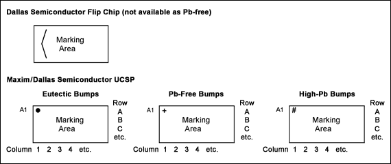
Figure 4. Flip chip and UCSP logo template
You can learn about the UCSP superscript codes in the More Information section of the Quick View page. In some cases, this information is also included in the data. For reverse lookup, for example, to determine the package of the device from the top mark, you can use the top mark code function on the website or download the complete top mark table 13 and use the search function to identify the corresponding device. The superscript code is for UCSP containing 12 solder balls. The larger UCSP has enough space for detailed information such as all models and date codes. Table 2 shows the trademarks used by Maxim devices.
Table 2. Typical Maxim UCSP trademarks
| Maxim Brand | Legend | ||||||||||||||||
|
| ||||||||||||||||
| |||||||||||||||||
| |||||||||||||||||
| |||||||||||||||||
|
The trademark types in Table 3 also apply to Dallas Semiconductor's flip chip and UCSP. The laser marking is very small and requires a magnifying glass to see clearly. Dallas Semiconductor's flip chip uses a similar method for the smallest device. The 2-digit device code (also called the serial code) is followed by the die version number. This method does not require a cross reference list.
Table 3. Typical Dallas Semiconductor flip chip and UCSP trademarks
| Dallas Semiconductor Brand | Legend | ||||||||||||||
|
| ||||||||||||||
| |||||||||||||||
|
Reliability of wafer-level packaged devices Wafer-level packages (flip chip and UCSP) represent a unique package shape, which is different from packaged products that use traditional mechanical reliability testing. The reliability of the package is mainly related to the user's assembly method, circuit board materials and use environment. Users should seriously consider these issues when considering the use of WLP models. Working life test and anti-moisture performance test must be carried out, these performances are mainly determined by the wafer manufacturing process.
The mechanical pressure performance is a major problem for WLP. After flip chip and UCSP are directly soldered, they are connected to the user's PCB, thereby alleviating the internal pressure of the lead structure of the packaged product. Therefore, the integrity of the soldered contacts must be considered. Dallas Semiconductor's wafer level package assembly guide 14 provides detailed information on circuit board layout considerations, assembly process flow, solder layer screen printing, component layout, reflow temperature profile requirements, epoxy packaging, and visual inspection standards. Application note 189115 introduces Maxim's limited specifications and details of test data. The quick browsing page provides reliability information for Maxim devices; the company website provides reliability reports for Dallas Semiconductor devices, see Table 4.
Table 4. Reliability report of Dallas Semiconductor flip chip and UCSP
| Device | Applicable Reliability Reports with URL |
| DS2431 | http: //Dallas-8in_CSP20_RDL_3x3.pdf |
| DS2401 | http: //DS2401.pdf http: //Dallas_Backgrind_FC-RDL.pdf |
| DS28E01 | http: //Dallas-8in_CSP20_RDL_3x3.pdf |
| DS1804 | http: //Bump%202%20layer%20underfill.pdf http: //Bump%202%20layer%20w-redistribution%20underfill.pdf |
| DS1845 | http: //Bump%202%20layer%20underfill.pdf http: //Bump%202%20layer%20w-redistribution%20underfill.pdf |
| DS2406 | http: //Bump%202%20layer%20underfill.pdf http: //Bump%202%20layer%20w-redistribution%20underfill.pdf |
| DS2411 | http: //DS2411A1Bump-8in.pdf |
| DS2415 | http: //Bump%202%20layer%20underfill.pdf http: //Bump%202%20layer%20w-redistribution%20underfill.pdf |
| DS2417 | http: //Bump%202%20layer%20underfill.pdf http: //Bump%202%20layer%20w-redistribution%20underfill.pdf |
| DS2430A | http: //FlipChip_RDL_8in.pdf |
| DS2432 | http: //Dallas-8in_CSP20_RDL_3x3.pdf |
| DS2433 | http: //Bump%202%20layer%20underfill.pdf http: //Bump%202%20layer%20w-redistribution%20underfill.pdf |
| DS2502 | http: //DS2502Bump.pdf http: //Dallas_Backgrind_FC-RDL.pdf http: //FlipChip_RDL_8in.pdf |
| DS2760 | http: //FlipChip_RDL_8in.pdf |
| DS2761 | http: //FlipChip_RDL_8in.pdf |
| DS2762 | http: //FlipChip_RDL_8in.pdf |
Conclusion The current flip chip and CSP are still new technologies and are in the development stage. Measures being improved will use back-side laminate cladding (BSL) technology to protect the passive side of the die from light and mechanical impact, and improve the readability of laser markings under light. In addition to BSL, there will be a smaller die thickness, keeping the total height of the assembly unchanged. The Maxim UCSP dimensions (see Table 1) illustrate the product packaging in February 2007. According to the general development trend of the industry, these sizes may be further reduced. Therefore, the designer should determine the package size of the design from the respective package outline before completing the circuit board layout, which is very critical. In addition, it is also important to understand the composition of the solder ball die WLP alloy, especially when the device is not declared or marked as a lead-free product. Some devices with high-lead solder balls (Pb95Sn5) have passed the lead-free circuit board assembly reflow soldering process test and will not significantly affect their reliability16, 17. Devices using eutectic SnPb solder balls require similar eutectic SnPb soldering surfaces, so they cannot be used in lead-free assembly environments.
Refer to Analog Devices, Application Note 617 (PDF, 414kB) National Semiconductor, Application Note 1281 (PDF, 225kB) National Semiconductor, Application Note 1412 (PDF, 828kB) STMicroelectronics, Application Note 1235 (PDF, 328kB) STMicroelectronics, Application Note 2348 ( PDF, 333kB) Maxim Integrated Products, FCHIP package drawing Maxim Integrated Products, UCSP package drawing Dr. Philip Garrou, IEEE Components, Packaging and Manufacturing Technologies Society, Semiconductor International, October 2000, http: //? Layout = articlePrint & articleID = CA47705 Michael Töpper , Fraunhofer Institute for Reliability and Microintegration (Fraunhofer-IZM); Philip Garrou, IEEE Components, Packaging and Manufacturing Technology Society, Semiconductor International, October 2004, http: //? Layout = articlePrint & articleID = CA456679 M. Töpper, V. Glaw , K. Zoschke, O. Ehrmann, H. Reichl, Fraunhofer IZM-TU Berlin Microperipherics Center, Advancing Microelectronics-January / February 2006, http: // (PDF, 6.73MB) Amkor Technology, Wafer Level Packaging Data Sheet (PDF, 164kB) Maxim Product naming convention Topmark Cross-Reference Table (PDF, 265kB) (200 pages or more) Maxim Wafer Level Package Installation Guide Wafer Level Package (WL-CSP) package foundation is assembled using a lead-free (Pb) assembly process High-lead DS2502 flip-chips are used to install lead-containing DS2761 flip-chips in the lead-free assembly process. * The term "eutectic" is used in the metallurgical industry to describe the composition of more than two materials and a certain concentration relationship at the eutectic point alloy. When a non-eutectic alloy changes from a liquid state to a solid state, one material of the alloy crystallizes at a certain temperature and another material crystallizes at another temperature. The eutectic alloy solidifies at a temperature point and has a clear melting point. This is in contrast to non-eutectic alloys, which have melting ranges similar to plastics (extracted from http: //).
Washing machines are very common in every family. Banshen washing machines, with high quality, good design and best service. Many products have been sold to over 30 countries. After many years of developing, banshen washing machines are getting better and better.
Our well-equipped facilities and excellent quality control throughout all stages of production enable us to guarantee total customer satisfaction. Besides, we have received CE, CB, RoHS and CCC certifications.
As a result of our high quality products and outstanding customer service, we have gained a global sales network reaching America, Asia, Europe, Africa, the Middle East and other countries and regions.
If you are interested in any of our products or would like to discuss a custom order, please feel free to contact us. We are looking forward to forming successful business relationships with new clients around the world in the near future.
Portable Washer,Baby Washing Machine,Twin Tub Washing Machine,3Kg Portable Twin Tub Washing Machine
Ningbo Banshen Electric Appliance Co., Ltd , https://www.banshendq.com