Design scheme of wireless communication transceiver module based on FPGA
1 Introduction
In recent years, with the rapid development of semiconductor process technology and design methods, the design of system-on-chip SOC has developed rapidly, which has become a hot spot in the industry. However, due to the relatively long development cycle, high cost and high risk of SOC product design, it is very sensitive to changes in the market, which makes the development process of SOC in the fields of consumer electronics, automotive electronics and industrial design still slow. At the same time, today's manufacturing processes can provide more and higher-speed logic, faster 1 / O, and lower-cost new-generation programmable logic devices. Field programmable gate arrays (FPGAs) have entered embedded applications. In the field, high-performance FPGAs are no longer limited to the introduction of system bonding logic, and can also be used as an SOC platform. In the past, due to performance, only application-specific integrated circuits (ASICs) or application-specific standard products (ASSPs) could meet the corresponding requirements. Not only that, due to the field programmable features of FPGA, it has become an industrial design platform with more flexible and extensive development prospects.
FPGAs can be easily modified, changed, or fixed, or when users need to upgrade and cooperate with market development to create future derivatives. This trend is more apparent in the design of industrial wireless communications. When considering issues such as time to market, implementation flexibility, and future obsolescence, using FPGA as a dedicated chip design is an optimal project implementation.
Communication based on Morse signals is the earliest wireless communication method of mankind, and it is still used in maritime mobile communications, aviation mobile communications, broadcasting, and satellite communications. Due to the traditional nature, economy and effectiveness of Morse code signal communication, it is still dominant in maritime mobile communications, especially Morse communication between ships and ships, ships and shores, shore and ships More than 80% of the total business.
The automatic processing of MORSE code signal based on PC has been realized, but in maritime mobile communication, it is still subject to some objective conditions, lacking general convenience and flexibility. This article starts with the special chip design technology based on FPGA platform, analyzes and designs a design scheme of Morse code wireless communication transmission module, and simulates and verifies the design.
2 Programmable logic circuit design method
Based on the basic design method of programmable logic circuit, one is the traditional system hardware circuit design method, which is a bottom-up (bottom-up) design method. The other is the EDA (Electronic Design AutomaTIon) hardware circuit design method that began to emerge in the 1980s.
With the development and development of large-scale application-specific integrated circuits, in order to improve development efficiency and increase the inheritance of existing development results, as well as shorten development time, various emerging EDA tools began to appear, especially the hardware description language HDL (Hardware DescripTIon The emergence of Language) has caused a huge change in the traditional hardware circuit design method. The emerging EDA design method adopts a top-down design method. The so-called top-down design method is to proceed from the overall requirements of the system, gradually refine the design content from top to bottom, and finally complete the overall design of the system hardware. The top-down design of system hardware circuits using language is generally divided into three levels: the first level is the behavior description, which is a description of the mathematical model of the entire system; the second level is the register transfer description RTL, also known as Data flow description; The third layer is logical synthesis.
Using the logic synthesis tool, the program described by the RTL method can be converted into a file-level netlist represented by basic logic elements, and the synthesis result can also be output as a logic schematic diagram, which means that the logic synthesis result is equivalent to manual design When the hardware circuit, the logic electrical schematic diagram of the system is drawn according to the system requirements. Then simulate the logic synthesis result at the gate level and check the timing relationship. If everything is normal, then the hardware design of the system is basically over. The process of designing system hardware from top to bottom is shown in Figure 1.
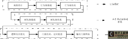
Figure 1: The process of designing system hardware from top to bottom
After the gate-level netlist is generated by the logic synthesis tool, when the hardware design is finally completed, there are two options: one is the manufacturing process of converting the netlist into the corresponding ASIC chip by the automatic routing program, and the custom ASIC chip; The second is to convert the netlist into corresponding PLD programming code points, and use the PLD device to complete the hardware circuit design.
3 FPGA-based Morse code functional structure design
Morse code is regarded as a data mode with key control. The time of "stroke" in Morse code is 3 to 4 times longer than that of "point". Different combinations of "point" and "stroke" form different lengths. Morse code. Different Morse codes indicate different telegraph symbols. The sender first translates the text to be transmitted into a telegram symbol, and then sends it out using a telegraph machine, and the recipient translates the received telegram symbol into a message, so as to achieve the spread of wireless text. At present, the solution to realize the automatic processing of the Morse code signal by the method of microcomputer simulation, so that the wireless Morse code signal data enters the computer information network has been solved. Morse code, and then send the Morse code signal through the parallel port of the microcomputer. When receiving, the Morse code signal is recognized by the audio card first, and finally decoded into ASCLL code by software. This method is relatively expensive and lacks in actual application. Convenience and flexibility.
According to the requirements of the marine communication business, the function of the MORSE code processing system is defined as: First, it automatically encodes according to the instructions and sends the MORSE code in serial. That is, the ASCLL code can be automatically extracted according to the instruction, and then the ASCLL code is automatically encoded into the Morse code, and the edited MORSE code is automatically serially output. Second, it automatically receives and decodes the Morse code according to the instruction, and sends the ASCLL code into the system. That is, the Morse code input is automatically received according to the instruction, and the received Morse code is automatically decoded into the ASCLL code. Store the ASCLL code to the target address or send it to the system for processing.
Through the study of the characteristics of Morse code, we can see that in designing the Morse code transceiver module, there must be a serial asynchronous communication module that can receive and send Morse code information frames. First of all, the serial communication module must have the ability to automatically send Morse code under the control of the command, and also have the ability to recognize and receive the MORSE code, because the start and stop bits of the Morse code serial asynchronous frame are different from ASCLL codes are serial asynchronous frames, and different Morse codes have different serial frame lengths. The second is the decoding and encoding of Morse code, because the computer core uses ASCLL code as the information exchange code.
From this, as long as the serial communication submodule with the function of receiving and sending MORSE code serial information frames, and with the function of decoding and encoding Morse code, and embedding it on the system bus, it is directly processed by the computer The MORSE code becomes possible. According to this analysis, the design requirements of the Morse code transceiver module can be obtained. On the one hand, the Morse code can be decoded into parallel ASCLL code from the serial receiving end, on the other hand, the parallel ASCLL code can be encoded into serial Morse code. code. Therefore, the internal block diagram of the Morse code transceiver module based on FPGA designed in this paper is shown in Figure 2.
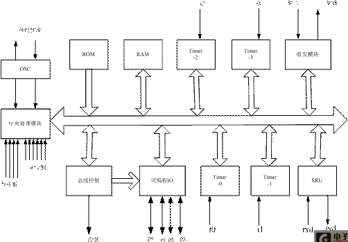
Figure 2: Block diagram of the internal composition of the Morse code transceiver module based on FPGA
The main functional modules of the processing system are:
Core control module Bus control module Programmable interrupt processing module Programmable parallel I / O interface (P0, P1, P2, P3) Programmable serial interface unit (SIU) Programmable timer counter 0 ~ 3 (TImer0 ~ TImer3) Programmable Morse code asynchronous transceiver moduleThe interrupt processing module has 4 external interrupt sources (int0 ~ int3) and 6 internal interrupt sources (TF0 ~ TF3, T1 / R1, mT1 / mR1), SIU is the system's universal serial interface, it has 4 working modes, Working mode 1 ~ 3 is the working mode of Universal Serial Asynchronous Receiver / Transmitter (USART). When SIU works in working mode 1 or 3, Timer1 is its baud rate generator.
4 Simulation and verification
Design verification includes functional simulation, timing simulation and circuit verification. Simulation verification is often achieved with the help of EDA development tool packages or special simulation tool software provided by the third party. Circuit verification also requires the development of a verification platform, which is also a difficult and unavoidable task for the design of system-level chip verification platforms.
This article selects MaxPlusII of Altera as EDA development tool, MaxPlusII compiler supports functional simulation (pre-simulation) and timing simulation (post-simulation). After completing the source code (VHDL) design input, if you want to perform functional simulation, under MaxplusII / Compile, select the Functional SNF Extractor command under the Processing menu to open the functional simulator netlist file (SNF) extractor and then compile Simulation; if you want to perform timing simulation (timing) simulation, you must select the Timing SNF Extractor command in the Processing menu under MaxPlusII / Compile to open the timing simulator netlist file extractor to compile and simulate.
Circuit verification is the process of device programming and testing. For conventional chip design, after the timing simulation is completed, the simulation software can generate data files for device programming. For EPLD / CPLD, it is to generate a fuse map file, that is, JED file. For FPGA, it is to generate a bitstream data file (Bitstream Generation), and then download the programming data to the corresponding specific programmable device, and then Carry out circuit testing of the actual environment.
In this paper, the CLK frequency is 25MHZ, and the baud rate is 25M / 16 = 1562500bps. When the character '7' is sent and the send command is executed, the process of data transmission will be started, and the ASCLL code value of the character '7' will be sent to the ASCLL code transmission buffer. Through the Simulator simulator of MaxPlusII, the timing simulation is verified and the research results As shown in Figure 3. It can be seen from the figure that the "2 long strokes" and "3 points" output by the serial signal terminal correspond to the Morse number '7' after the lookup table, which proves that the data transmission is correct. In addition, when the data output is completed, it is set to a high level immediately, that is, an interrupt signal mTI is generated, and the transmission of the character '7' takes about 10us.
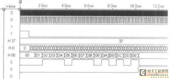
Figure 3: Simulation verification data
5 Summary of innovations
The innovation of this article is to propose a FPGA-based wireless communication transceiver module. Taking the Morse code that is an important position in maritime communication as an example, the digital coding method of Morse code is studied, and a large number of analysis and design The experimental simulation realizes the transceiver module for processing Morse code based on FPGA. The simulation results also verify that the digital coding method of Morse code designed in this paper is correct and feasible, and the operation is reliable.
This Bluetooth Karaoke Microphone Speaker is designed for music singing fans. This Karaoke Microphone Speaker is the most wonderful microphone. This portable Microphone speaker combines microphone, KTV echo and louder speaker in one. The Good Speakerphone for Home Office connects Mobile phone/tablet/computer by Bluetooth easily, you can enjoy singing at anywhere and anytime. With cable, it supports singing recording at the same time. At home party, this Portable Karaoke Speaker can increase the enjoyment of life, you can sing song freely with your family and friends, and you can use this Wireless Microphone systems record your songs and submit to some sing APP to get high popularity. Also people can use this Bluetooth Conference Speakerphone make speech practice to add your public presentation ability. It is a good present for your family and friends.


Microphone Speaker
Microphone Speaker,Portable Mic System,Portable Mic Speaker System,Portable Wireless Mic System
Shenzhen New Wonderful Technology Co., Ltd. , https://www.sznewwonderful.com