Amplifier circuit diagram of mc1496 analog multiplier
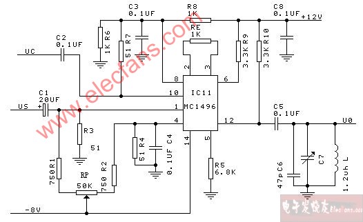
The amplitude modulator circuit composed of MC1496 is shown in the figure
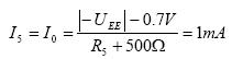
The carrier signal UC is input from the ux terminal through the high-frequency coupling capacitor C2, and C3 is the high-frequency bypass capacitor, so that pin 8 is grounded. The modulation signal UΩ is input from the uy terminal through the low-frequency coupling capacitor C1, and C4 is the low-frequency bypass capacitor, which makes pin 4 grounded. The amplitude modulation signal U0 is output from pin 12 single-ended. The device adopts dual power supply mode, so the 5-pin bias resistor R5 is grounded, and the static bias current I5 or I0 of the device can be calculated by formula (7-4), namely
Connect negative feedback resistor RE between pins 2 and 3 to extend the linear dynamic range of UΩ of the modulated signal. RE increases, and the linear range increases, but the gain of the multiplier decreases accordingly.
Resistors R6, R7, R8 and RL provide a static bias voltage for the device to ensure that each transistor inside the device
Working in the amplified state, so the selection of resistance should meet the requirements of formula (7-1), (7-2). For the circuit parameters shown in Figure 7-3, the static (UC = 0, UΩ = 0) bias voltage of the measurement device is
u8 u10 u1 u4 u6 u12 u2 u3 u5
6V 6V 0V 0V 8.6V 8.6V -0.7V -0.7V -6.8V
R1, R2 and the potentiometer RP form a balance adjustment circuit. Changing the RP can enable the multiplier to realize the amplitude modulation of the suppressed carrier or the amplitude modulation of the carrier. The operation process is as follows:
(1) Suppress carrier amplitude modulation
The carrier signal UC (t) is input at the ux terminal, the frequency fC = 20.945MHz, and the peak-to-peak UCP-P = 40mV. uy
Input the modulation signal UΩ (t) at the terminal, the frequency fΩ = 1kHz, first make the peak-peak UΩP-P = 0, adjust RP, make the output
U0 = 0 (in this case, U4 = U1), when UΩP-P is gradually increased, the amplitude of the output signal U0 (t) gradually increases, and finally the amplitude-modulated signal that suppresses the carrier as shown in Figure 7-4 (a). Since the internal parameters of the device cannot be completely symmetrical,
Cause the output to leak signal. Pins 1 and 4 are connected to resistors R3 and R4, respectively, to better suppress carrier leakage signals and improve temperature performance.

(a) Suppression of carrier wave amplitude modulation (b) Amplitude wave with carrier regulator Figure 7-4 AM wave output by multiplier
MC1496 / MC1496B / MC1496P pdf datasheet mc1496 Chinese data (analog multiplier)
Fiber optic transceivers, is a short twisted-pair electric signals and optical signals over long distances to swap the Ethernet transmission media conversion unit, in many places also known as the photoelectric Converter (Fiber Converter). The product is generally used in the actual network environment where the Ethernet cable cannot be covered and the optical fiber must be used to extend the transmission distance. For example, high definition video image transmission of monitoring security engineering; It has also played a big role in helping to connect the last kilometer of fiber optic lines to the WAN and beyond.

Fiber Optic Media Converter, Fiber Media Converter, Optical Fiber Transceiver
NINGBO YULIANG TELECOM MUNICATIONS EQUIPMENT CO.,LTD. , https://www.yltelecom.com