With the rapid development of the communications market, the complex tree structure for clock distribution has been widely used. A clock tree is necessary in order to feed signals to many nodes that are distributed by clocks and other nodes designed to transmit data (through many different functional design combination units with digital time domain accuracy). Since a large number of clocks are required to time multiple nodes in the system, it is imperative to generate these timing clocks within a strict and very precise and limited window time.
Currently, these windows are measured in picoseconds. As the number of nodes to which signals must be fed increases and the timing window into which clocks must be placed rapidly decreases, designers must understand the characteristics of the devices used to complete the generation, frequency multiplication, and transmission of these clock signals. Many of today's clock signal generation and transmission products include PLLs, which further increases the complexity of the timing system. These PLLs enable designers to retime clocks that lag or lead, eliminate the propagation delays that occur during the transmission of long-distance clock signals, and generate clock signals that are phase-locked to a reference clock and have different frequencies.
While using PLL to obtain these clock control capabilities, it also brings about the deterioration of PLL reliability. It is necessary to understand the deterioration of the signal quality generated by all PLL-based clock processing elements and provide certain tolerances. The noise added by the PLL to the clock signal processed by it cannot be completely eliminated. This noise is often tolerated, and the components in the clock tree that contain the PLL can be configured to control so that they can The noise generated is controlled and the overall clock tree performance is far above the acceptable minimum.
The noise accumulated by the PLL on the clock signal transmitted or generated by it is jitter. In electrical terms, jitter refers to the time deviation of a specified clock point (usually a rising or falling edge of a pulse under a specified voltage) relative to its absolute expected point. This jitter has traditionally been divided into two major categories. The first type is short-term jitter, which is measured according to the displacement of the time point relative to its ideal position in adjacent clock cycles. The common term used for this parameter is cycle to cycle jitter.
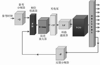
Figure 1 Phase-locked loop (PLL)
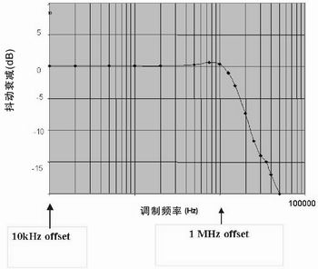
Figure 2 Typical jitter transfer function curve of zero delay buffer
Another type of jitter is measured over a long period of time. One term used for this type of jitter is long-term jitter. The term with higher frequency and accuracy is long-term periodic jitter. In this field, a length of time (in cycles or seconds) must be specified to limit the sampling period of the event to produce measured values. If there is no restriction on the sampling period, the event may drift in an uncertain position. Therefore, the measurement period for measuring the incidence of the event must be set and explained in order to specify the specific method of measurement more accurately. For a specific application, it is usually related to the stability that the pulse edge must have within a certain period.
In the process of establishing a clock tree with a reasonable value, it is inevitable that PLL-based clock processing elements need to be connected in series. In this case, it is necessary to understand the mutual influence of the jitter caused by each component, and more importantly, it is necessary to understand the jitter content of all final component clocks generated by the clock tree. This article will make a comprehensive discussion from the perspective of principle and function.
When engineers plan to adopt a design that includes multiple PLL clock processing elements in series, they often face two sources of information. The first source of information is the traditional knowledge possessed by RF designers. Although there are many introductions to RF-based PLL design, they often involve circuits that mix two PLL-based signals to generate a sum or differential clock. Moreover, they generally do not have picosecond timing restrictions like digital designs. There are a lot of theoretical information available in the field of digital clocks, but what designers need is some empirical information or evidence to transform this application problem into a clear and predictable point of view, that is, to specify the design goals and should Where to focus design time and resources to achieve a sound design solution.
This article will study the performance obtained by a special and typical experiment using 5 series PLLs. Although we do not recommend that you adopt a design scheme in which 5 PLL devices are connected in series, this scheme is specifically adopted here to emphatically reflect the various adverse effects that designers care about.
When studying clock processing components based on PLLs, the first thing to understand is their role in the clock signals that must be passed through them. Figure 1 shows a typical ZDB (zero delay buffer) element and its components.
The most important for electrical performance is the series element group consisting of phase detector, error amplifier, charge pump and loop filter. For an input reference clock signal, these components act as a second-order low-pass filter. Figure 2 shows the jitter and frequency transfer functions and the bandwidth response of the device used in this example.
This is a graph of the input-output transfer function. It indicates the gain (and loss) of any input frequency to the component. Please note that the input frequency (either the frequency itself can be loaded on the input reference signal) will be transmitted and amplified by the combined stage of the loop filter and phase detector. The frequency above 1.5MHz roll-off point (as well as the frequency component of the complex wave) will be attenuated by this filtering action and thus suppressed when passing through the device.
In order to analyze and explain the effect of the PLL clock processing device on the clock signal passing through it, the following will study the noise existing on the clock signal as it passes through several successive stages in three different views.
The first is the frequency domain view. This view will use a spectrum analyzer to observe a graph of power level as a function of frequency to understand how this noise propagates in the system.
The second is a long-period jitter view. Here you can observe how the output clock works for a long period of time, and the actual frequency distribution of these periodic changes. The measurement will use a TIA (Time Interval Analyzer) to show the correlation between the amount of occurrence (total) and frequency.
The third is the modulation domain view. In this view, you can observe the frequency change from cycle to cycle (CC) in a series of medium-length cycles or between adjacent cycles. It will show the presence of pulses or instantaneous frequency (jitter) as well as a medium-term view.
The devices used in this article have the following data sheet characteristics:
· 200ps CC jitter · 1MHz PLL loop bandwidth There is a fairly flat noise layer on both sides of the reference carrier frequency. The width and slope of the carrier frequency sweep depends on the video performance and resolution bandwidth settings of the spectrum analyzer. It is important to pay attention to the flatness of the noise layer relative to the rising and falling edges of the reference clock pulse, because we are concerned about the variation of this flatness between processing stages.
It can be seen from FIG. 2 and related explanations that the PLL-based clock device functions as a low-pass second-order filter in the frequency domain. In the process of studying the spectrum content of each successive stage, it can be clearly found that the noise within the pass band of the loop filter is transmitted among the successive stages and amplified step by step. In fact, for the output of the second and subsequent stages, there is a definite peaking of the spectral energy transferred through these. It corresponds to the slight peaking at the edge of the pass band shown in FIG. 2. The second concern is the noise layer outside the passband of the device. Please note that even after 5 levels of gain, the noise layer is still relatively close to the level of the input signal (top and bottom) of the waveform amplitude.
For frequencies close to the reference frequency, the PLL-based clock device does act as a low-pass filter. Low frequency (near carrier frequency) energy and signal components will easily pass through the device. This means that the low frequency energy (in terms of performance, it will be converted to a low frequency and the slow movement or drift of the output frequency) will be transmitted and amplified as the signal passes through successive processing stages. Who will control its final value (the deviation from the input reference to the first level expressed in units of frequency) depends almost entirely on the bandwidth of the device and any other attempts to suppress it between the various levels of the clock tree.
The second view we will study is the long-term or periodic jitter view.
The first thing to note is that the density distribution is essentially a Gaussian function. This supports the known fact that random jitter caused by actual noise inside the component or inherent white noise in the input signal will appear on the signal as a highly predictable Gaussian distribution spread (frequency modulation) effect. The second thing to note is the effect of this noise on the total amplitude of the clock signal at multiple processing stages, as well as the accumulation and spread of noise as it passes through each additional processing stage (distributed over a wider frequency range).
It should be noted that these frequencies are close to the fundamental frequency. This is consistent with this article's point of view because it shows that noise and energy components close to (or within) the passband of the device are not only transmitted by the device that amplifies it. Also, since the noise (jitter) is close to the operating frequency of the device, the rate of occurrence of jitter is very slow. Based on this fact, the overall effect is to make the second stage track the error of the first stage signal, the third stage track the errors of the first stage and the second stage, and the last stage track the accumulation of all the processing stages preceding it ( Additive) error.
The period-to-period jitter of the high-frequency domain of the clock is accumulated between all levels, and its increment is very small. In some systems, it may even decrease as it passes certain processing stages. The reason for this is that cycle-to-cycle jitter occurs between adjacent cycles of the clock. In this example, the fundamental frequency of the clock is 106.25MHz. In order for the waveform to respond to an impulse noise (short-term and high-frequency part of the frequency content of the spectrum), its frequency will have to be above 100 MHz. Otherwise, the effects of noise will be spread over many cycles. Because the loop bandwidth of the device is narrow, such energy is filtered through the edges of the band-pass curve, so it is not easy to propagate between stages. In a precisely designed system, wide-bandwidth components can be used to deliver this artificially modulated interference as the required EMI suppression spread-spectrum modulated signal (at a cycle rate of less than 35kHz). Therefore, in order to reduce the cumulative high-frequency jitter of the system, a very narrow bandwidth PLL device can be used to effectively filter out this and other high-frequency noise before applying the target system equipment.
Summarize what is explained in this example. First, as the signal passes through successive PLL-based clock processing stages, the low-frequency noise contained within the band-pass characteristics of the PLL-based device will propagate and be amplified and accumulated. If the system being designed is a time base (clock) that requires long-term stability and is not adversely affected by the instantaneous turn-off frequency, then the method of connecting PLL clock processing devices in series will have minimal impact on the system. Due to the long-term Gaussian balance process, any short-term changes will eventually be balanced.
Therefore, if two to three consecutive clocks are used to time the events in the system very tightly, this is not a problem, because the accumulation time of the long-period jitter is too long, so it is impossible to form enough Errors that affect the events that occur. In these applications, the common practice is to time the dynamic memory, CPU, and other devices that exchange data with them. Here, although the stability of three consecutive clocks in a RAS-CAS-READ cycle has a crucial impact in terms of moments, long-period changes over a span of 1,000 cycles have little effect.
On the other side of the spectrum, it can be seen that very fast (far beyond the PLL bandwidth used by the device) jitter does not pass through a system with multiple PLL-based clock devices. The cycle-to-period jitter that exists on the output of any device is mostly the same as the jitter to the device under test. This means that devices that are very sensitive to cycle / frequency changes in adjacent or very close cycles in their clock pulses are expected to work well with series-connected, PLL-based clock device trees. The main negative impact on applications using PLL-based serial clock device trees occurs in specific data applications in which an input data stream has many consecutive data bits that are divided into very special and scattered time windows. In such applications, when restoring data from a data stream, the long-term shift of the clock generated by a long PLL-based element tree may cause the clock signal to fall outside the desired unit time domain.
Dc Linear Actuator,Linear Actuator,Linear Actuator 12V,Electric Linear Actuator
Changzhou Sherry International Trading Co., Ltd. , https://www.sherry-motor.com