Abstract: The article gives the specific method of designing ISO / IEC15693 card reader using TI's latest RF transceiver chip RI-R6C-001A, combined with a microprocessor, and also introduces the communication protocol and ISO of RI-R6C-001A / IEC15693 standard.
1 Overview
The development of IC cards has gone through the process from memory cards to smart cards, from contact cards to non-contact cards, and from short distance to long distance. For contact cards (as defined in the ISO / IEC 7816 standard), the card reader must be in contact with the card's contacts to exchange information with the card, so there are shortcomings such as serious wear, vulnerability to contamination, short life, and time-consuming operation. In order to solve the above problems, people began to adopt contactless card technology.
Contactless cards are also called RF cards or proximity cards. It uses radio modulation and card reader for information exchange. Radio frequency identification? RFID? Technology is an automatic identification technology that has emerged since the 1990s. It uses wireless radio frequency for non-contact two-way communication to achieve identification and data exchange. 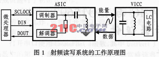
RFID is different from contact identification technologies such as magnetic cards and IC cards. The identification between the electronic tags and readers of the RFID system can be completed without physical contact, so it has the characteristics of multi-target recognition and moving target recognition.
At present, the card defined by ISO / IEC 10536 is called a close-coupled card; the card defined by ISO / IEC 14443 is a near-coupled card (PICC), the corresponding card reader is abbreviated as PCD; and the card corresponding to ISO / IEC 15693 is a remote-coupled card ( VIC), the corresponding card reader is abbreviated as VCD. VICC has a farther card reading distance (about 1m) than PICC. Both use 13.56MHz operating frequency, and both have an anti-collision mechanism.
2 Hardware design
Figure 1 shows the working principle diagram of a radio frequency reading and writing system, which is mainly composed of ASIC and VICC.
2.1 The working principle of ASIC circuit 
For the radio frequency reading and writing system shown in Fig. 1, the physical layer protocols of VCD and VICC communication specified in ISO / IEC 15693-2 can all be realized by the ASIC chip RI-R6C001. The user uses the synchronous serial interface (SPI) and complies with ASCII The communication requirements can realize the read and write operations of VICC. The communication interface between MCU and ASIC has three lines: SCLOCK, DIN, and DOUT, which respectively represent the clock line, data input line, and data output line. The clock line is bidirectional, controlled by the MCU when sending data, and controlled by ASIC when receiving data. The ASIC latches data on the rising edge of the clock. In addition to the data output function during data reception, DOUT also has the function of characterizing the internal FIFO of ASIC. DOUT with internal pull-down, usually low level. During data input, when the 16-bit FIFO register of ASIC is full, the DOUT line will automatically jump to a high level until the FIFO register is empty, and the DOUT line will jump to a low level again. While DOUT is high, the input data is invalid. In addition to the communication line, the system also has an M_ERR line, which is used to characterize the data conflict when reading multiple cards at the same time. Similarly, the M_ERR line also has an internal pull-down, which is usually low, and this line will rise to high level during conflict.
There are three modes of operation of ASIC: normal mode, register mode and direct mode. In the direct mode, the MCU directly faces the RF signal processing, which is more complicated, so this mode is generally not used. Normal mode and register mode are standard digital signal operations. The difference lies in the different parameters that specify the operation of the chip (for example, whether the radio frequency protocol, modulation method and transmission rate used are specified in the command sequence or set by the register of). Each command in the normal mode contains the parameters used by the command, but the register mode command sequence does not contain these parameters, but is determined by the value written in the register in advance. If the RI-R6C-001A chip works normally, the time register must be initialized after the ASIC is powered on. 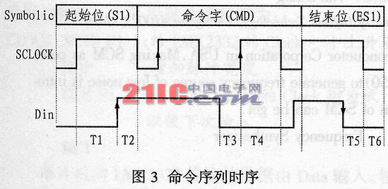
2.2 VICC-Tag-it transponder
VICC-Tag-it transponders are fully compatible with ISO / IEC 15693 standard protocol. The VICC-Tag-it transponder has an internationally uniform and non-repeating 8-byte (64 bit) unique identification internal code (UNIQ IDENTIFIER, referred to as UID). Figure 2 is a schematic diagram of the UID unique identification internal code format, in which the first 1-48 bits total 6 bytes are the manufacturer's product code; the first 49-56 bits one byte is the manufacturer code (ISO / IEC 7816-6 / AM1), The highest byte is fixed at "EO"; 8-bit AFI (application identification number) and 8-bit DSFI (data storage format) are used to identify the characteristics of the card and specific applications. There are 2kbit EEPROM in the card, divided into 64 blocks, 32 bits per block. Each block can be locked to protect the data from being modified. AFI, DSFID and 32 blocks are all readable and writable, used to store user data. VICC-Tag-it uses a carrier frequency of 13.56MHz and works in the "READER TALKS FIRST" mode, which is a question-and-answer mode. The card has an anti-collision mechanism, which can read multiple cards at the same time without causing conflicts. In particular, it should be pointed out that there is no logic encryption circuit in VICC-Tag-it, and it is impossible to realize the cryptographic function. It is this point that restricts the application of VICC-Tag-it in other fields that require higher confidentiality.
3 Communication protocol
The sequence of commands sent to ASIC must comply with the ASIC communication protocol and ISO / IEC 15693-3 specifications.
3.1 Command structure
Figure 3 shows the timing diagram of the command sequence of the system. In normal mode, the command sequence structure of the system is as follows:
| Start bit (S1) | Command word (CMD) | data | End bit (ES1) |
Start bit (S1): The communication start bit between the transceiver and the microprocessor. When the SCLOK bit remains high, a rising edge will be generated at the DIN (see Figure 3).
Command byte: It is used to specify the relevant parameters during the communication between ASIC and VICC. If the end is 30H, it means that the radio frequency protocol supported by the system is ISO 15693 (selected from 256), adopts FM modulation, the modulation rate is 10%, and the returned data baud rate is 6.67kb / s. Note: The order of sending the command byte is high-order first, namely: MSB FIRST.
Data: The content of the data field is specified by 15693-3? This data is generally sent to TAG.
End bit (ES1): The communication end bit between the transceiver and the microprocessor. When the SCLOK bit remains high, a falling edge will be generated at the DIN (see Figure 3).
Usually in register mode, the command byte is 1 bit, and this bit is 1.
The general format of the ISO 15693-3 command is as follows:
| Start bit (S1) | FLAGS | Order number | Command content | CRC16 | End bit (ES1) |
In the ISO 15693 command sequence, FLAGS is used to specify the existence of certain optional fields in the command content. Since S1 and ES1 already exist in the ASIC command sequence, you only need to take out the contents of the FLAGs, command number, command content, CRC16 and other fields in the ISO 15693 command sequence and fill in the data fields in the ASIC sequence and then package. The sending order of the data field is low-order first, namely: LSB FIRST.
3.2 Response structure
Figure 4 shows the response timing of VICC. The general format of the VICC response is:
| Start bit (S2) | FLAGS | Response content | CRC16 | End bit (ES2) |
The start bit S2 is used to indicate the start of the VICC response data. Its definition is that when SCLOCK is high, DOUT generates a rising edge (see Figure 4). The end bit ES2 indicates the end of the VICC response data. It is defined that when SCLOCK is high, DOUT generates a falling edge (Figure 4). 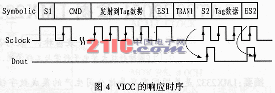
4 Conclusion
Considering that the order in which the command byte (8 bits) is sent is MSB FIRST, and the other data are LSB FIRST; and "S1101111011 01000ES11" is the initialization sequence of the time register; at the same time, during the command transmission process, the bidirectional clock SCLOK line is MCU control, therefore, the clock line must be switched before receiving the VICC response to hand over the control to ASIC control. For FIFO management, the level of DOUT must be detected when sending each bit. When DOUT is high, it stops sending until DOUT returns to a low level. After sending the command byte, it should be properly delayed to facilitate the correct action of ASIC, and the anti-interference ability of the circuit should be considered. For bytes such as FLAGs, command serial number, and command content specified in ISO 15693-3, CRC16 verification should also be performed. Regarding the anti-collision problem, a "binary search" algorithm can be used and Manchester encoding is selected. To implement this algorithm, a set of commands are required and processed by the transponder. At the same time, the transponder must have a unique serial number (UID). For example, there are two cards in the magnetic field, and their UIDs are: "E00700000234D1E1" and "E00700000234D2D8" Then, using the command to query the card number of the current magnetic field can solve the collision problem.
Heavy Duty Connector, also known as HDC, is widely used in construction machinery, textile machinery, packaging and printing machinery, tobacco machinery, robots, rail transit, heat runner, electric power, automation and other equipment requiring electrical and signal connection. The international advanced features of Heavy Duty Connectors in structural design and material usage make the connectors outstanding in electrical performance.The reliability of the electrical connection system can not be achieved by the traditional connection method.
Cold Crimp Contact is the main contact of heavy duty connector, used for connect wire and pin to realize the electrical connection; cold Crimp Contact surface is gold plated and silver plated option for anti corrosive purpose.
Cold Crimp Contact,Crimp Contact Pin,Crimp Connector Housing,Heavy Duty Connector Crimp
Suzhou WeBest Electronics Technology Co.Ltd , https://www.webestet.com