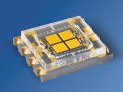
The chip is the core component of the LED. At present, there are many LED chip manufacturers at home and abroad, but there is no uniform standard for chip classification. According to power classification, there are high power and medium and low power; if classified by color, it is mainly red, green and blue; According to the shape classification, it is generally divided into two kinds of wafers and wafers; if classified by voltage, it is divided into low voltage DC chip and high voltage DC chip. Compared with domestic and foreign chip technology, foreign chip technology is new and domestic chip weight production is not heavy technology.
Substrate materials and wafer growth technology are key Currently, the key to the development of LED chip technology is substrate materials and wafer growth technology. In addition to traditional sapphire, silicon (Si), and silicon carbide (SiC) substrate materials, zinc oxide (ZnO) and gallium nitride (GaN) are also the focus of current LED chip research. Currently, sapphire or silicon carbide substrates are widely used in the market to epitaxially grow wide bandgap semiconductor gallium nitride. Both of these materials are very expensive and are monopolized by large foreign companies. The price of silicon substrates is higher than that of sapphire and carbonization. The silicon substrate is much cheaper and can produce larger substrates, improve the utilization of MOCVD, and increase the yield of the die. Therefore, in order to break through the international patent barriers, Chinese research institutes and LED companies started researching silicon substrate materials.
However, the problem is that the high quality bonding of silicon and gallium nitride is a technical difficulty for LED chips. The technical problems such as high density of defects and cracks caused by the large mismatch between the lattice constants and the thermal expansion coefficient have long impeded the field of chips. development of.
Undoubtedly, from the perspective of the substrate, the mainstream substrates are still sapphire and silicon carbide, but silicon has become the development trend in the chip field in the future. For China, where the price war is relatively serious, silicon substrates have more cost and price advantages: the silicon substrate is a conductive substrate, which not only reduces the die area, but also eliminates the need for dry etching of the GaN epitaxial layer. In addition, the hardness of silicon is lower than that of sapphire and silicon carbide, and some costs can be saved in processing.
Currently, the LED industry mostly uses 2-inch or 4-inch sapphire substrates. If silicon-based GaN technology is used, at least 75% of raw material cost can be saved. According to estimates by Sanken Electric Co., Japan, the cost of manufacturing a large-size blue GaN LED using a silicon substrate will be 90% lower than that of a sapphire substrate and a silicon carbide substrate.
Differences in chip technology at home and abroad are significant in foreign countries. First-class companies such as Osram, U.S. Puri and Sanken have achieved breakthroughs in large-size silicon substrate gallium nitride-based LED research. Philips, South Korea’s Samsung, LG, and Toshiba’s international LEDs The giants also set off an upsurge of research on gallium nitride-based LEDs on silicon substrates. Among them, in 2011, Puri developed high-efficiency GaN-based LEDs on 8-inch silicon substrates, achieving a luminous efficiency of 160 lm/W that is comparable to that of top-level LED devices on sapphire and silicon carbide substrates. In 2012, OSRAM succeeded in producing 6-inch silicon-based GaN-based LEDs.
In contrast, in mainland China, the breakthrough point of LED chip technology is mainly to increase production capacity and large-size sapphire crystal growth technology, in addition to the successful mass production of 2-inch silicon substrate GaN-based high-power LED chips by Jingneng Optoelectronics in 2011. China's chip companies have no major breakthrough in the research of silicon-based gallium nitride-based LEDs. At present, LED chip companies in mainland China still focus on production capacity, sapphire substrate materials, and wafer growth technologies. Sanan Optoelectronics, BDO Runda, Tongfang shares Most mainland chip giants also made breakthroughs in their production capacity.
Office Window Cleaning Robot apply to office, home, hotel, shop and so on. You can saves the labor, money, energy using smart window robot clean office. Office window robot is suitable for frame glass (rimless glass is also ok), door, wall. The noise is only 48dB when you use window robot clean office, giving you a quite environment.
Window Cleaning Robot Reviews beat HOBOT window robot, we become to Top sale . window cleaning robot test very good before leaving facotry. Welcome to place order ws - 960 window cleaning robot.

Specifications of robotic window cleaner:
Dimensions: 285*136*100mm
Weight: 0.92kg
Cleaning speed: 3′/㎡
Applicable Area: ≤100㎡
Working height: No limited
Anti-drop control: UPS / safety rope
Detection window frame: Auto recognition
Operation: Automatic / remote control
Alarm prompt function: Voice alarm
If there is anything confusing you, please feel free to contact me for further discussion. Our factory is in Shenzhen, China. Welcome to visit. It will be our honor to see you.
Office Window Cleaning Robot
Office Window Cleaning Robot,Building Window Cleaning Robot,Window Cleaning Robot Reviews,Office Building Window Cleaning Robot,Window Cleaning Robot Reviews,Window Cleaning Robot For Office
Zhengzhou Bangmi Smart Technology Co., Ltd. , https://www.cleanwindow-robot.com