Lighting is an area that is closely related to human life and an important aspect of energy consumption, accounting for about 20% of the world's total energy consumption. As a new high-efficiency solid-state light source, LED (Light EmitTIng Diode) is widely used in indoor and outdoor lighting, landscape design, and indicator lights due to its high efficiency, environmental protection and long life. LED lighting has quickly become one of the most popular fourth-generation electric light sources, and has become the development direction of the future lighting industry.
In addition, in order to meet the needs of actual production and power saving, LEDs usually need dimming. The realization of the dimming circuit not only saves energy and reduces waste, but also avoids the LED working in an overload state for a long time, thereby improving the operating efficiency and life of the LED. This paper studies the operating state of LEDs in different dimming modes by studying power electronic switching converters and dimming strategies, and realizes an efficient combined dimming strategy.
1 Flyback drive circuit analysis
The isolated flyback circuit has the advantages of minimum device, low cost, high power density, electrical isolation, easy realization of multiple outputs, and protection against voltage. It is suitable for low Power Supply devices below 150 W, while LED lighting generally uses low power. Power supply unit. In this paper, the flyback circuit is used as the main circuit, and UC3842 is used as the control chip. UC3842 is a fixed-frequency current-type control chip with few external components and an oscillation frequency of up to 500 kHz. The control is simple and the peripheral circuits are mature. The circuit schematic is shown in Figure 1.
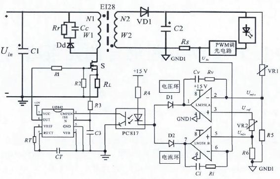
Figure 1 Flyback constant current drive circuit
Due to its steep volt-ampere characteristics, LEDs are typically driven by constant current. This article uses a dual loop to control the constant current output. As shown in Fig. 1, the current signal is converted into a voltage signal by a current sampling resistor Rs, compared with a given Uref-i value, and adjusted by PI, and the current error signal is formed as an internal current loop through the optocoupler isolation, and the switch The current is compared, and then a PWM wave is formed by the UC3842 internal comparator to control the opening and closing of the switching tube. When the current reference value is constant, the circuit works to reach a steady state, that is, a constant current output. The Uref-i value can be changed by adjusting VR2 to achieve the dimming effect. In addition, in order to prevent output overvoltage, a voltage loop is added to the feedback link, and the output voltage limit value is changed by adjusting VR1. The reference voltage Uref in the figure is supplied by the TL431 with a reference voltage of 2.5 V.
2 dimming strategy analysis
The brightness of the LED changes approximately proportionally with the change of the forward current IF. When the average value of the forward current is changed, the magnitude of the light output can also be changed accordingly. There are two common ways to change the IF size, as shown in Figure 2.
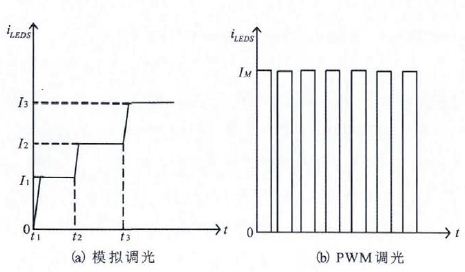
Figure 2 Two ways to change the forward current
In Fig. 2(a), the luminous flux output is changed by continuously adjusting the current flowing through the LED at different times, and the current flowing through the LED is continuous; in Fig. 2(b), an Im value is given first. By controlling the current with a different duty cycle Ddim, the current flowing through the LED:
In the formula, Ton is the on-time in one cycle Tdim of the dimmer switch. Thus, the dimming effect can be achieved by adjusting the dimming duty ratios Ddim and Im.
According to the way of changing the current, the dimming circuit can be divided into analog dimming and PWM dimming.
2.1 Analog dimming
The analog dimming mode can be divided into switching amplitude variation AM dimming and linear dimming, and its circuit control schematic is shown in Figure 3. The amplitude variation dimming is shown in Figure 3(a), which generally has two methods:
1 Fix the size of the reference voltage Uref-i and change the size of the sampling resistor Rs. In order to reduce the system power consumption, Rs generally takes less than 1 Ω, and the potentiometer of about 1 Ω on the market is relatively rare; 2 the current sampling resistor remains unchanged, and the magnitude of Uref-i changes linearly, that is, the current reference value changes. This can reduce the power consumption on the resistor, and is simple and convenient. Linear dimming is to use the power tube operating in the amplification area as a dynamic resistor. As shown in Figures 3(b) and (c), it is divided into two types: parallel type and series type. At this time, the main circuit operates in the constant voltage mode, and the circuit current is adjusted by changing the resistance of Q1. Analog dimming can avoid noise generated during dimming, no flicker, and is simple and convenient. However, the converter is always in continuous operation, and the loss of the system is relatively large. On the other hand, the optical characteristics such as the color temperature and the light effect of the LED during analog dimming will change with the current, and in the case of strict requirements on color temperature and the like. The method is limited.
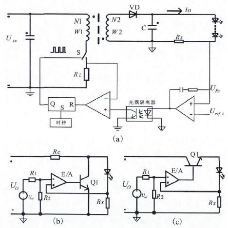
Figure 3 Analog dimming diagram
2.2 PWM dimming
PWM dimming can accurately control the current flowing through the LED, the dimming range is wider, the color temperature does not drift, and the efficiency of the LED driver is high. The disadvantage is that noise is easily generated during dimming. The PWM dimming frequency is generally above 200 Hz to avoid LED flashing. The dimming scheme is shown in Figure 4. In the output load, a switching transistor is connected in series, and the LED current is repeatedly turned on and off by the single-chip output PWM pulse to adjust the luminance of the light.
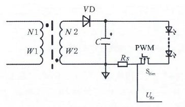
Figure 4 PWM dimming diagram
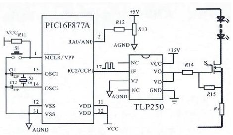
Figure 5 Schematic diagram of dimming PWM generation circuit
The PWM module is generated by the 8-bit microcontroller PIC16F877A manufactured by Microchip. The crystal oscillator of the MCU is 4 M, and the dimming frequency fdim is set to 250 Hz. The data after AD acquisition is converted into a given value of the duty cycle, and the PWM wave outputted by the single chip is amplified by TLP250 and used as a PWM signal for driving the dimming MOS transistor. The circuit schematic is shown in Figure 5.
Since the flyback circuit cannot operate in the no-load state, when the no-load output current is 0, the output voltage will quickly reach the voltage limit value, so Im is the maximum current of the circuit during PWM dimming. When performing PWM dimming, first adjust the voltage loop and current loop so that the maximum operating current of the circuit is the rated current Im, and PWM adjustment of Im, then iLEDS=DdimIm.
2.3 Combined dimming
Combining analog dimming with PWM dimming complements each other and is especially useful in applications where both analog dimming and PWM dimming are required. According to the characteristics of the circuit and the practical application, a dimming scheme combining two dimming methods is proposed.
(1) Change Im to perform mixed dimming based on PWM dimming. When the dimming switch Sdim is turned off, the output voltage is the voltage limit value Uo-set, and during the turn-on time of Sdim, the output portion constitutes a first-order zero-input response. LED model UO=Uturn-on+Rled&TImes; IO, the equivalent circuit diagram is shown in Figure 6. After DdimTdim's on-time, the output voltage is:
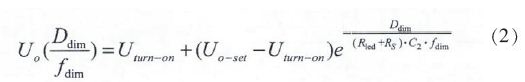
Let Ddim be adjustable in the range of 0.3~1, Uo-set takes 30 V, Uturn-on takes 25 V, fdim takes 250 Hz, output capacitance takes 2000 μF, Rled is 7 Ω, then Uo>29 V. Therefore, at the time when Sdim is turned on, Uo basically keeps the voltage limiting value unchanged, and the current is the maximum value Im under the limit. At this time, adjusting the current loop has no effect, and changing the voltage limit value by continuously adjusting the voltage loop, thereby changing Im to achieve the dimming effect.
(2) The second dimming scheme: the LEDs are connected in parallel in two ways, one with analog dimming, and one with PWM dimming. The two-way dimming diagram is shown in Figure 7. The output voltages of I and II are both Uo, then the I channel is dimmed by analog mode; the Im of II is the current value under voltage Uo, and the current flowing through II is changed by changing the duty cycle. Light. If the load of the two paths is the same, then Io=I1+I2≈(1+D)I1.
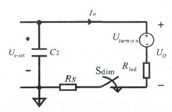
Figure 6 Output equivalent power when the dimming switch is closed
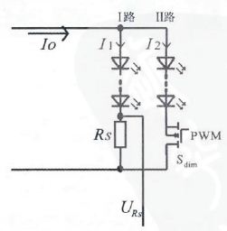
Figure 7 Two-way dimming diagram
600V DC Electronic Load can be switched quickly between different values in the same operating mode, including CC dynamic mode, CV dynamic mode, CR dynamic mode and CP dynamic mode, CC/CR high speed dynamic mode up to 50kHz. This function is suitable for transient test of power supply, test of battery protection characteristic and battery pulse charging etc. Dynamic mode test has continuous mode, pulse mode and toggle mode.
Additionally , programmable dc electronic load can also have 200V DC Electronic Load and 1200V DC Electronic Load for more options.
kindly check below features for your reference:
â— Flippable front panel and color touch screen allow convenient access and operation
â— Provides four kinds of basic working mode such as CV/CC/CR/CP, and CV+CC/CV+CR/CR+CC complex operating modes
â— Adjustable current slew rate, adjustable CV loop speed
â— Ultra high precision voltage & current measurement
â— OCP/OPP testing function
â— 50kHz high-speed CC/CR dynamic mode
â— 500kHz high-speed voltage and current sampling rate
â— Timing & discharging measurement for batteries
â— Short circuit test mode
â— Auto mode function provides an easy way to do complicated test
â— Dynamic frequency sweep function for determining worst case voltage peaks*
â— Non linear load mode function makes the simulated loading current more realistic*
â— Supports external analog control function*
â— V-monitor/I-monitor
â— LED load simulation function
â— Full protection: OCP, OPP, OTP, over voltage and reverse alarm
â— Up to 20 units master/slave parallel control
â— Front panel USB interface supports data import and export
â— SCPI language and standard rack size make it ideal for ATE System integration
â— Smart fan control with lower noise and better for environment
â— Multi versions to meet the cost performance and different applications
* Only professional electronic load units support these functions
600V DC electronic load
600V DC Electronic Load,programmable dc load,adjustable electronic load,programmable DC electronic load
APM Technologies (Dongguan) Co., Ltd , https://www.apmpowersupply.com