At the end of the year and the beginning of the year, when we look back at the development of the industry in 2014, IoT (Internet of Things) and Big Data (Big Data) are the two most talked about in the scientific and technological circles in 2014. They are also on the list of the 2014 TOP10 hot search rankings published by the IEEE. However, by opening their gorgeous coats, we are seeing a surprising development of the various advanced high-performance and ultra-low-power semiconductor technologies behind them.
Power consumption becomes a key design challenge for HPC and Networking
There is no doubt that IoT has promoted the development of low power, but this is only one aspect of the problem. On the other hand, ubiquitous mobile devices have generated huge data torrents, and more and more remote monitoring systems and embedded systems have produced huge data sets, some of which only flow through the network. Some do fine-grained analysis, such as finding a car license that kidnapped a child from the surveillance image stream, or a Higgs boson that appears only once a month. Big data forces us to dramatically increase network and computing bandwidth. However, while accelerating for the data center, the issue of power consumption is at hand.
"Most people's deep understanding of energy consumption is limited by the limitations of mobile devices' power life. This gives us the illusion that only mobile devices are power-sensitive applications, in fact, in data such as In the areas of high-performance computing (HPC) and networking (Networking), such as the center, the power consumption requirements are even more demanding.†Mr. Chen Chen, Marketing Manager of Fujitsu Semiconductors, at the annual China IC Design Industry Conference The China Mainland and Hong Kong Integrated Circuit Industry Collaborative Development Summit Forum (ICCAD Summit) said.
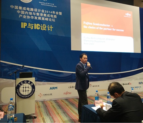
Figure 1. Mr. Chen Boyu, Manager of Fujitsu Semiconductor Marketing, speaks on ICCAD
Unlike the fixed power of the mobile phone, the power of the data center is always on, and every chip in the whole room is working all the time, and the pressure on the entire power supply system, including the heat dissipation system, is enormous. According to statistics: when the server is less than 10,000 units, the annual power consumption is about 35 million kWh (electricity is a secondary factor); when the server is less than 100,000 units, the annual power consumption is about 350 million kWh (electricity is an important factor); When the number of servers is less than 500,000 units, the annual electricity consumption is about 1.75 billion kWh (electricity is the main cost); when the server is less than 1 million units, the annual power consumption is about 3.5 billion kWh (electricity is TOP1 cost).
It is very different from the consumer application. In the communication field, the power consumption of each board is required. Only by meeting the power consumption requirements of each board, the power consumption of the entire system can reach the standard. “In the field of high-performance applications, the design scale of the billion gates has increased the complexity of the chip, how to optimize the power consumption, and achieve the performance requirements. This is especially important in large-scale design.†Chen Boyu pointed out .
Multiple approaches to powering high-performance designs
Today's high-speed, low-power designs feature designs with more than 700 million gate-level circuits and operating frequencies in excess of 2 GHz. Therefore, designers need to carefully evaluate how to define and optimize the low-power strategy for the entire chip in the shortest design cycle, and think about how to make the package design meet the ultra-high power consumption.
Large-scale layout design can help designers meet the challenges of high-speed and low-power design, as shown in the following figure. 2 Fujitsu Semiconductor's collaborative design technology optimizes all aspects of chip, IP, and package-to-board design. To optimize performance, through planning, designing, modeling, and analyzing all processes, Fujitsu Semiconductor uses a predictable power network architecture and uses hierarchical power network analysis to optimize power network design. And minimize the power consumption of the entire chip. The low noise chip architecture is designed to withstand more than 300 watts of power.
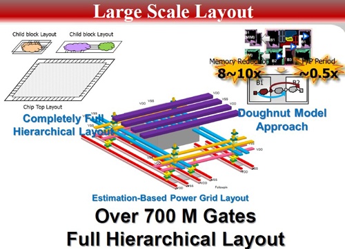
Figure 2. Large-scale layout design can help designers address high-speed, low-power design challenges
In addition, it is worth mentioning that Fujitsu Semiconductor's unique ASV (Adapter Support Voltage) technology. As shown in Figure 3 below, this technology is used to monitor the speed of the process.
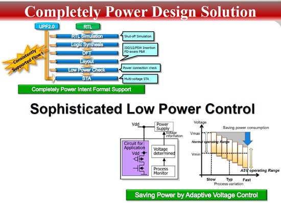
Figure 3. Full-power design solution addresses high-speed, low-power design challenges
Chen Boyu further explained: "Because the fab's process has fast (fast), slow (slow), and standard (typ) states, placing 'Process Monitor' on the chip allows us to read the parameters of the process, so that Knowing the size of the power supply, for example, if we read the faster process, it can help reduce the voltage, because the power is proportional to the square of the voltage, so reducing the voltage can reduce power consumption, ASV technology is like a spring, Pull the chip toward typ."
Again, high-performance packaging solutions are essential to address power challenges. Fujitsu Semiconductor is also a leader in the high-performance packaging market. During the development of these high-reliability packages, Fujitsu Semiconductor conducted rigorous simulations to optimize the technology prototype. As shown in Figure 4 below.
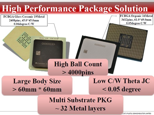
Figure 4. High-performance packaging solutions address high-speed, low-power design challenges
“Our spherical packaging technology supports more than 4,000 pin pins, and the package size on each side can reach 60mm. Our multi-layer substrate package design can support up to 32 layers. For BGA package, our unique metal TIM achieves ultra low Theta JC, Theta JC is less than 0.05 degrees and has been validated with the latest thermal resistance measurement technology. We are developing a new generation of 2.5 and 3D packaging technology for CPUs and servers.†Chen Boyu said.
Plant Factory LED Grow Light
Led grow light for herb, Led grow light full spectrum, Led grow lights, Led grow light bulb
Shenzhen Ri Yue Guang Hua Technology Co., Ltd. , https://www.ledlightinside.com