Application overview
The Advanced Driver Assistance System (ADAS) will see significant growth in the coming years. One of the main reasons is the increased awareness of safety and the increased customer demand for driving comfort. However, the most important reason is that the European New Car Safety Assessment Association (NCAP) has strengthened safety requirements, which will drive the installation rate of ADAS equipment from single digits to almost 100% next year. Therefore, a commercially viable solution is undoubtedly a top priority.
Vision-based ADAS can greatly improve driving safety in many ways. By installing a rear view/front view/side view camera and a vision processing ECU, multiple functions can be implemented to help the driver prevent risks in advance. Popular applications include route deviation warning (LDW), high beam low beam adjustment (HB/LB), traffic signal identification (TSR), parking assistance, rear view/rear look, collision avoidance, and more.
Program characteristics
To achieve this power consumption, Analog Devices has adopted a straightforward and special concept. This concept is based on two Blackfin cores, as the mass-produced ADAS system is adopting this architecture. However, algorithms that cannot be cost-effectively modeled by software have been implemented with hardware engines, resulting in a highly configurable visual processing unit toolbox. Analog Devices calls it the Pipeline Vision Processor (PVP), which is now part of the new ADSP-BF60x processor. Although low-power processing technology is employed, further innovation is needed to solve the most important power consumption problem in modern design. This method is an external memory (DDR2) interface. The lowest power consumption can be achieved by properly allocating processing power and making reasonable use of the appropriate amount of memory bandwidth. In addition, some hardware modules enhance the Blackfin architecture to meet functional safety requirements.
System requirements and design challenges
• Supports functional safety as required by ISO26262
• Ability to use in an application-oriented development environment
• Optimized visual processing library
• Helps design an overall system with short time to market and low risk
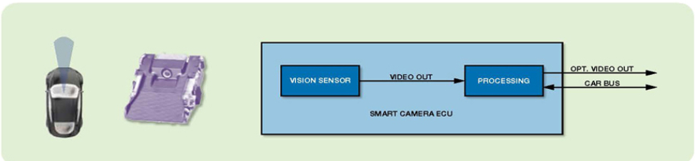
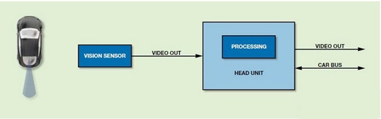
Main signal chain
1.ADAS camera - smart camera ECU
2.ADAS ECU - camera + central processing ECU
Related reference device
1.DSP
The dual-core ADSP-BF606 Blackfin processor is optimized for a wide range of industrial, instrumentation, medical, and consumer electronics applications that require complex control and signal processing tasks while maintaining extremely high data throughput. Specific features include a high-performance enhanced infrastructure, large on-chip memory, and a feature-rich set of peripherals with extended connectivity options including USB 2.0 HS OTG, two 10/100 Ethernet MACs, and a Mobile Memory Interface (RSI). In addition, the ADSP-BF606 processor features features for safety-critical applications, including CRC for memory protection, parity and ECC protection in internal memory blocks, and fault management unit.
Functional Block Diagram for ADSP-BF606 Blackfin Processor
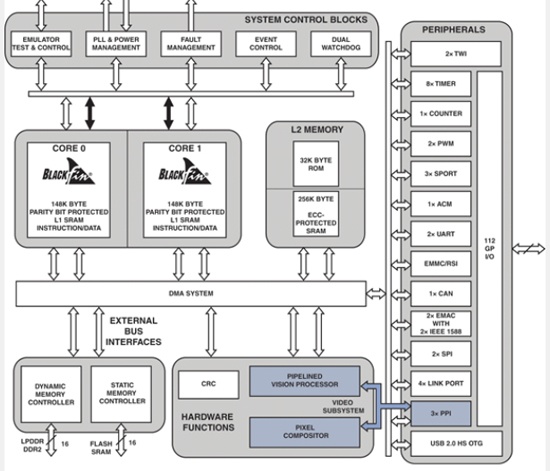
Details: ADSP-BF606 BLACKFIN dual-core processor for high-performance digital signal processing applications
2. Video decoder
The ADV7280/ADV7280-M are feature-rich, single-chip, multi-format video decoders. The ADV7280/ADV7280-M automatically detects standard analog baseband video signals and is compatible with NTSC, PAL and SECAM global standard signals in composite, S-video and component video formats. The ADV7280 converts analog video signals into a 4:2:2 component video data stream that is compatible with the 8-bit ITU-R BT.656 interface standard. The ADV7280-M converts analog video signals into an output video stream compatible with the Mobile Industrial Processor Interface (MIPI®) CSI-2 (8-bit YUV). The ADV7280/ADV7280-M's analog video inputs support single-ended signals. The ADV7280 provides four analog inputs, while the ADV7280-M provides eight analog inputs. The ADV7280 and ADV7280-M support I2P conversion. The ADV7280/ADV7280-M are programmed through a 2-wire serial bidirectional port (I2C compatible) and fabricated in a 1.8 V CMOS process. The decoder offers LFCSP package options, making it ideal for space-constrained portable applications.
Functional Block Diagram for ADV7280
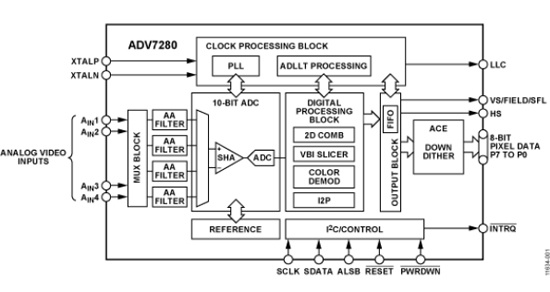
Details: ADV7280 10-bit, 4x oversampling SDTV video decoder
3. Video Encoder / DAC
The ADV7125 (ADV®) is a single-chip, three-channel, high-speed digital-to-analog converter with three high-speed, 8-bit video DACs with complementary outputs, a standard TTL input, and a high-impedance, analog output current source. It has three independent 8-bit wide input ports. It only works with a single +5 V/+3.3 V supply and clock. The ADV7125 also has other video control signals: composite SYNC and BLANK, as well as power-saving modes.
Functional Block Diagram for ADV7125
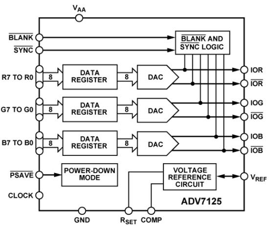
Details: ADV7125: 330MHz, 3-Channel, 8-Bit, High Speed ​​Video DAC
4.RGB-CVBS converter
The AD725 is a very low cost general purpose RGB to NTSC/PAL encoder that converts red, green and blue component signals into corresponding luminance (baseband amplitude) and chrominance (subcarrier amplitude and phase) in accordance with NTSC or PAL standards. signal. At the same time, the two outputs are combined on-chip to provide a composite video output. All three outputs are available for independent use and are twice the standard signal level required to drive a 75 Ω reverse terminated cable.
Functional Block Diagram for AD725
Details: AD725 RGB to NTSCPAL encoder
5. Video amplifier
The ADA4851-1 (single channel), ADA4851-2 (dual channel) and ADA4851-4 (quad) are low cost, high speed, voltage feedback, rail-to-rail output op amps. While these devices are less expensive, they still provide excellent overall performance and a wide range of features. The −3 dB bandwidth and high slew rate of 130 MHz make these amplifiers ideal for many general-purpose high-speed applications. The ADA4851 family is designed to operate from a +3 V to ±5 V supply. These devices have a single-supply capability and the input signal can be extended to 200 mV below the negative supply rail and 2.2 V from the positive supply rail. The amplifier's output swing is within 60 mV of either rail.
ADA4851-1 pin configuration
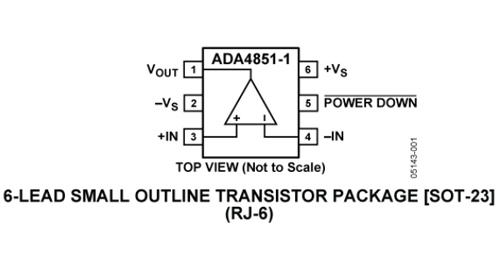
Details: ADA4851-1 Low Cost, High Speed, Rail-to-Rail Output Operational Amplifier
6. Temperature sensor
The ADT7311 is a high precision digital temperature sensor in a narrow 8-pin SOIC package. It has a bandgap temperature reference and a 16-bit ADC for temperature monitoring and digital conversion with a resolution of 0.0078°C. The default ADC resolution is set to 13 bits (0.0625°C). The ADC resolution is user programmable and can be changed via the serial interface.
Functional Block Diagram for ADT7311
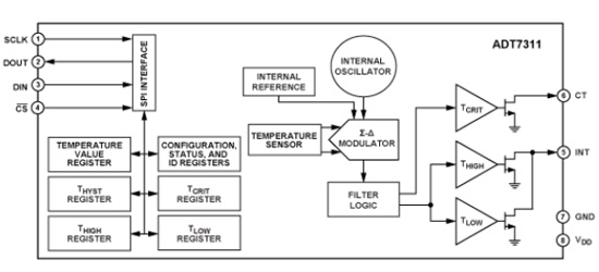
Details: ADT7311 Automotive Application High Precision Digital SPI Temperature Sensor
Design resources
Hardware development board
· BF60x Standard Evaluation Board and Expansion Board · Front View ADAS Development Kit (please contact ADI Sales Department)
BF60x DSP integrated development environment: CCES
Standard software module
· ADAS Visual Analysis Toolbox (AVAT) · Blackfin Image Processing Toolbox (IPTBX)
· 2D Graphic Toolbox (GFX2D)
Visual ADAS framework and algorithm reference code
· LDW, FCW, TSR, HBA, PD functions
Datacard Printers Cleaning Kits
Datacard Dcc Leankit Cleaning Kit,Datacard Cleaning Kit With Roller,Datacard Complete Cleaning Roller,Adhesive Cleaning Sleeves
Miraclean Technology Co., Ltd. , https://www.mrccleanroom.com