The 555 Timer is a mid-scale integrated device that combines analog and digital functions. Generally called 555, which is made by bipolar process, is called 7555 in CMOS process. In addition to single timer, there is corresponding dual timer 556/7556. 555 timer has wide power supply voltage range, which can be 4.5. Operating at V~16V, the 7555 can operate from 3 to 18V with an output drive current of approximately 200mA, so its output is compatible with TTL, CMOS or analog circuit levels. The 555 timer has low cost and reliable performance. It only needs several external resistors and capacitors to realize pulse generation and conversion circuits such as multivibrator, monostable trigger and Schmitt trigger. It is also widely used as a timer in instrumentation, household appliances, electronic measurement and automatic control.
The outer lead of the 555 timer is arranged as shown in the figure. The function is shown in Table 6-1. It consists of two upper and lower voltage comparators, three 5kΩ resistors, one RS flip-flop, one discharge transistor T and a power output stage. The inverting input 5 of the comparator C1 is connected to 2/3 Vcc (also referred to as the control voltage terminal) of a voltage dividing network composed of three 5 kΩ resistors, and the non-inverting input terminal 6 is a threshold voltage input terminal. The non-inverting input of comparator C2 is connected to 1/3Vcc of the voltage divider resistor network, and the inverting input terminal 2 is the trigger voltage input terminal for starting the circuit. The outputs of the two comparators control the RS flip-flops. The RS flip-flop is set with a reset terminal 4, and when the reset terminal is at a low level, the output 3 is at a low level. The control voltage terminal 5 is the reference voltage terminal of the comparator C1, and the reference voltage of the comparators C1 and C2 can be changed by changing the voltage value of the control terminal by an external component or a voltage source. When not in use, it can be connected to the ground. 01μF capacitor to prevent interference voltage introduction. With a supply voltage range of +4.5 to +18V and an output current of 100 to 200mA, the 555 can directly drive small motors, relays and low-impedance speakers.
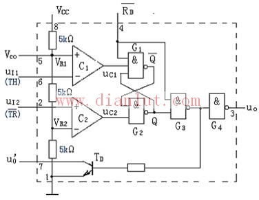
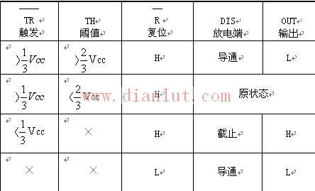
Table 6-1 555 chip function table
RAM/RFM electric heating capacitors
RAM/RFM Electric Heating Capacitors
Electric Heating Capacitor,Film Heating Capacitor,Electric Capacitor Bank,Induction Heating Capacitors
YANGZHOU POSITIONING TECH CO., LTD. , https://www.yzpst.com