Through which process technology measures in the chip manufacturing process, can the chip luminous intensity and light extraction efficiency be improved?
The brightness of the LED mainly depends on the epitaxial method and the quality of the epitaxial. Different methods in the chip manufacturing process can also improve some light intensity, that is, improve the external quantum efficiency, but to a limited extent. The most common method now used is the surface roughening process. The principle of roughening is to increase the light-emitting area. The method is applicable to yellow, green, Puhong, and Puhuang. Epitaxial wafers of GaPa substrates, etc., and infrared LEDs can also be used. This method can generally be increased by 30%.
Another method is to cover an AR coating. Since the refractive index of the LED crystal is relatively high, when the light is directed toward the crystal surface, refraction is generated at the interface between the crystal and the air. If the refractive index of the crystal is assumed to be N1, the incident angle is θ1, and when the refractive index of air is N2 and the angle of refraction is θ2, as shown in Fig. 1:

figure 1
According to the law of refraction, you can get:
NIsin θ1=N2sin θ2 (1)
It is known from the formula (1) that when θ2=90°, θ1 is called the incident critical half angle, which is represented by θC, that is,
θC=arcsinN2/ N1 (2)
Obviously, when θ1>=θC, the light is totally reflected inside the crystal. If a medium refractive index dielectric layer is plated between the LED crystal and the air, the critical angle θC can be increased. For example, N1=3.3 of GaP, if there is no dielectric layer, the critical angle θC=17.7 degrees. After covering a layer of N2=1.66, the θC may increase to 30.3 degrees, and the light intensity can be increased by 2.5 times.
At present, the light extraction efficiency of the chip can be improved through the improvement of the process and structure, and the following effective methods are summarized:
(1) Transparent substrate technology
Usually, the substrate of the LED is made of GaAs material, but GaAs is a light absorbing material, and the light emitted by the LED is absorbed by it, which reduces the light-emitting efficiency. Therefore, after epitaxially forming a PN junction, the GaAs substrate is removed by etching, and then the light-transparent GaP is pasted on the substrate under high temperature conditions, so that the PN junction emits light through the metal substrate to reflect light efficiency. .
In this method, when the InGaAlP quaternary chip is fabricated, a layer of metal is first formed by a bonding method after removing the GaAs substrate.
The mirror-reflective layer is then pasted with the substrate, so that the light that is incident on the substrate is radiated to the light-emitting surface, so that the light-emitting efficiency of the chip is improved.
(2) Chip surface roughening method
Since GaN has a refractive index η1=2.3, which is quite different from the air refractive index η1=1, the remaining reflection critical angle is only
At 25°, most of the light cannot escape into the air, and the light output efficiency is low. For this reason, by changing the geometry of the interface between GaN and air, the critical angle of total reflection is increased, and the light extraction efficiency is improved, which is achieved by the method of roughening the surface of the chip. Figure 2 shows a schematic view of the light exit surface of the chip.

Figure 2 shows the light surface of the chip
(3) The inverted ladder structure of the chip. CREE has a chip that uses an inverted trapezoidal structure to increase the light intensity, as shown in Figure 3. Since the critical angle of the total reflection of the edge portion of the chip of this structure is increased, the photon escape rate is increased, and it can be emitted from the bowl cavity, thereby improving the light intensity and the light extraction efficiency.

image 3
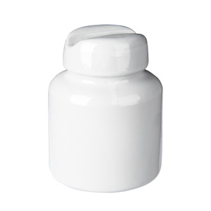
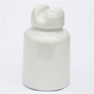
Telephone Line Insulators are pin-type ceramic Telephone Insulators , Vintage Telephone Insulators mainly in three models, M-1, M-2 and M-3. Glaze is usually supplied with white glaze. Telephone Wire Insulators parameters are as follows:
| MAIN DIMENSIONS AND STANDARD PARTICULARS | ||||
| Type | RM-1 | RM-2 | RM-3 | |
| Main Dimensions | H | 140 | 100 | 80 |
| h | 49.5 | 32 | 30 | |
| D | 86 | 70 | 60 | |
| d | 51 | 44 | 35 | |
| d1 | 22.5 | 18.5 | 13 | |
| R1 | 12 | 8.5 | 7 | |
| R2 | 4 | 3.5 | 3 | |
| Insulation Resistance | 50000 | 40000 | 20000 | |
| Leakage Distance | 298 | 215 | 15 | |
| Net Weight, Each Approx., kg | 1.1 | 0.5 | 0.5 | |


We warmly welcome friends both domestic and abroad to visit our company, if you have any questions, please contact with us directly.
Telephone Insulators,Telephone Line Insulators,Telephone Wire Insulators,Vintage Telephone Insulators
FUZHOU SINGREE IMP.& EXP.CO.,LTD. , https://www.cninsulators.com