As an important type of spread spectrum communication system, frequency hopping communication system has been widely used in military and civil communication fields due to its excellent anti-far effect and anti-interference ability. The frequency hopping communication method means that the carrier is controlled by a pseudo random code, and continuously and randomly hops, which can be regarded as multi-frequency frequency shift keying (MFSK) in which the carrier changes according to a certain rule. The frequency of frequency hopping communication is continuously changed by pseudo random code control. The frequency hopping pattern can be set to several thousand or even tens of thousands. Both ends of the transmitting and receiving ends can be hopped during the information transmission process as long as the hopping pattern is consistent and the hopping time is synchronized. Space frequency channel for frequency hopping communication.
In recent years, with the development of semiconductor technology and computer technology, modern signal processing chips such as DSP (Digital Signal Processor) and FPGA (Field Programmable Gates Array) have become more and more mature and widely used. The possibility of realization.
1 FPGA/DSP based frequency hopping system hardware architecture
The transmitting system of this frequency hopping communication system is shown in Fig. 1. The source information enters the DSP for channel coding; then the DSP enables the FPGA to control the DDS to generate a frequency hopping signal in the middle frequency band according to the coding result; finally, the mixer moves the signal frequency to the radio frequency, and is amplified by the high frequency amplifier and transmitted.
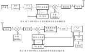
The receiving system is shown in Figure 2. The antenna amplifies the received signal through the high frequency amplifier, and mixes with the first local oscillator to generate a first intermediate frequency signal; the DDS is controlled by the DSP as the second local oscillator, and the same frequency hopping signal is hopped by the same frequency as the received frequency hopping signal. (But the frequency differs by an intermediate frequency), so that a fixed intermediate frequency is obtained, and the solution is de-jumped; then, the signal is subjected to intermediate frequency sampling, and the digital N-phase (NCO is located in the FPGA, controlled by the DSP) is used in the digital domain to realize digital demodulation; The result is channel decoding in the DSP, restoring the original information and sending it to the sink.
It can be seen that in the frequency hopping system, the FPGA is the carrier of the hardware logic, completes the mixing and filtering operations of the baseband signal sampling, and controls the external logic such as DDS and ADC; the DSP controls the internal logic of the FPGA and the logic such as DDS and ADC. The unit completes the transmission and reception of the baseband part of the frequency hopping communication system and a series of calculation tasks; the high-precision clock source provides the time reference for the whole system, and the internal phase-locked loop multiplier of the DSP, FPGA, DDS and other devices provides the main device for each device. clock.
2 Data communication design between DSP and FPGA
The interface between DSP and FPGA is shown in Figure 3.
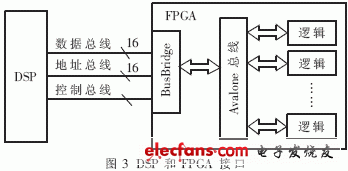
The logic design on the FPGA uses the SOPC design philosophy of OnChipBus+UserLogic. Among them, OnChipBus uses Avalon bus. The Avalon switch fabric is an interconnecting mechanism proposed by Altera Corporation to connect an on-chip processor and various peripherals in a programmable system-on-chip. It is a synchronous bus that contains complete bus arbitration logic and performs logic optimization for its own products. Particularly suitable for use on Altera FPGAs. However, the Avalon bus is not compatible with the external memory asynchronous interface timing of the C54x series DSP. For this reason, the Bus Bridge module is designed, and the DSP EMIF Slave Interface is connected to the EMIF of the DSP, which is mapped to the DSP IO space. The other side is Avalon. The Master Interface of the bus is connected to the Avalon bus to enable transparent transmission of data between the two buses.
The internal logic of the FPGA adopts a modular design idea. Each Logic includes three parts: AvalonSlaveInterface, RegisterFile, and UserLogic. Among them, AvalonSlaveInterface is the slave interface logic of AvalonBus; RegisterFile is the register group logic, which is mapped to the corresponding IO address space of DSP through Avalone bus; UserLogic is used to implement user logic, its function is completely determined by the contents of RegisterFile. Each module works independently, and communication between modules is performed through the on-chip bus, which increases design flexibility, is easy to maintain and expand, and can be integrated with the SOPC Builder tool.
3 Key module design of baseband part of frequency hopping system based on DSP/FPGA
3.1 Frequency hopping device design
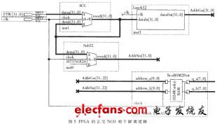
This design uses DDS as the frequency hopping device. The DDS can be thought of as consisting of an NCO and a high speed DAC. The NCO determines the frequency range, resolution, and phase resolution of the DDS output signal. It is mainly composed of a phase accumulator, a phase offset adder, and a cosine table. Its specific implementation is shown in Figure 4.
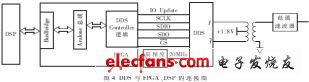
In order to adapt to the complex digital interface, the DDS Controller logic is designed in the FPGA to complete the conversion of all timing and data formats. The DSP can achieve all operations on the DDS only by reading and writing several registers in the DDS Controller. The output of the DDS uses a complementary current output, which is coupled through a transformer and passed through a low-pass filter to obtain a fundamental frequency signal.
Outdoor decorative LED mesh curtain screen is the perfect architectural decoration patterns in the daytime and night. And it becomes Led Display Screen to display image and video at night;Outdoor decorative Led Curtain Screen is ultra light weight design, which is easy to install. The convenient installation help everyone can install it easily by oneself. It can be packaged in one CMB which is save a lot in transportation. It is not only good for transport but also good for maintenance. Front and back maintain are available due to its special design;LED curtain mesh screen can be installed directly on the wall or glass. The hollow design makes permeability up to 70% which is conducive to ventilation and lighting. The exquisite appearance is good for decoration of shopping mall, hotel, office building and 5s shop etc;The frame shell save install material can be fixed easily. High-intensity sealed lamp with high quality up to IP67 protection level.
It is not only good for transport but also good for maintenance. Front and back maintain are available due to its special design.LED curtain mesh screen can be installed directly on the wall or glass. The hollow design makes permeability up to 70% which is conducive to ventilation and lighting. The exquisite appearance is good for decoration of shopping mall, hotel, office building and 5s shop etc.
Curtain Led Display,Transparent Curtain Led Display,Rgb Curtain Led Display,Soft Led Curtain Display Screen
Shenzhen Bako Vision Technology Co., Ltd. , http://www.rentalleddisplays.com