Abstract: With the large-scale promotion of mobile communication, mobile payment has become a hot topic of focus for all parties. This paper designs a dual controller reader for mobile payment system. The main controller mainly performs serial communication. The slave controller mainly accepts the command of the main controller and realizes the control of the card distance according to the transmitted Manchester code stream. . This design solves the problem that the card reader cannot receive low frequency data to some extent.
This article refers to the address: http://
With the popularization of mobile terminal communication technology, mobile phones are more than just simple communication tools. Entertainment and shopping have become popular services, and mobile payment has become one of the most representative businesses. Mobile payment, also known as mobile payment, refers to a service method in which a user uses a mobile terminal (mobile phone) as an electronic payment tool to implement consumer payment. Mobile payment makes a mobile phone a portable electronic wallet, which can realize electronic payment, identity authentication, Anti-counterfeiting, ticketing, advertising and other functions.
According to a report released in the "2014 China Internet Finance Development Report" jointly published by the China Internet Society and Xinhua News Agency "Financial World", the number of mobile payment users in China reached 125 million last year, a year-on-year increase of 126%. Mobile payment, online banking, and finance. The cumulative downloads of various related mobile applications such as securities exceeded 400 million times. In terms of e-commerce, the transaction volume of China's online retail market reached 28,63.72 billion yuan in 2014, a growth rate of 45%, and continued to maintain a high growth trend. The scale of mobile online shopping transactions reached 861.66 billion yuan, an increase of 229.3%. In terms of mobile payment, in 2014, the scale of third-party mobile payment transactions reached 776 billion yuan. After the explosive growth of 800% in 2013, it once again ushered in nearly 500% growth, and continued to maintain rapid development.
1 Mobile payment mode
At present, there are three main commercial application modes for mobile payment. The first one is to bind the user's mobile phone number and the payment account of the background user, and pay by SMS. The second is to use the client browser of GPRS or CDMA network to enter account information for payment. The third type is the contactless mobile payment mode, which is mainly applied to mobile payment applications such as public transportation and subway. At present, China's mobile payment field mainly adopts the third mode to realize payment. The contactless mobile payment model currently has three main schemes, namely dual interface SIMPASS, NFC, and RFID-SIM. The application modes and technologies of the three schemes are different. The SIMPASS solution has limited functions and must have an external antenna. Since the location of the SIM card of different mobile phones is also different, it needs to be adapted. NFC (Near Field Communication) scheme has high security and stable operation, and supports mobile phone peer-to-peer communication and active/passive communication mode. However, this solution needs to customize the mobile phone supporting NFC card. Currently, there are fewer mobile phones supporting NFC on the market, and it is difficult to promote. It is also very unfavorable for domestic telecom operators to control the industry. The RFID-SIM solution integrates the functions of the RF module, the antenna and the traditional SIM card into the SIM card. The user can also perform the contactless mobile payment transaction through the RF module while making a call or sending and receiving a short message. At the same time, the scheme adopts 2.4 GHz. Communication frequency, users only need to replace the SIM card, without replacing the mobile phone to achieve mobile payment consumption, high user acceptance, rapid card issuance, from the perspective of industrial chain control is the best choice for operators.
2 card reader hardware design
The frequency bands in which RFID systems operate are: 125 kHz, 13.56 MHz, 860-930 MHz, 2.45 GHz, and 5.8 GHz. Each frequency has its own characteristics and is suitable for different fields. Since the 2.4 GHz band can be used without authorization, the data transmission speed is fast and the metal is not affected much. The mobile payment can be realized by replacing the RFID-SIM card used. Therefore, this paper is mainly designed for the 2.4 GHz band.
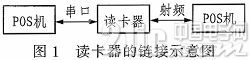
The mobile payment system consists of three parts: card reader, POS machine and RFID-SIM card. The link diagram is shown in Figure 1. The card reader is the link between the POS machine and the RFID-SIM card communication. It is mainly responsible for parsing the signals on the POS machine and the RFID-SIM card. The POS machine is mainly responsible for the processing of the terminal service, and is mainly responsible for sending or receiving information to the card reader; - The SIM card mainly accepts and processes the information sent by the card reader.
The hardware circuit module of the card reader is shown in Figure 2. It consists of four parts: power module, main controller module, slave controller module and RF transceiver module. Mainly responsible for high and low frequency signal transmission and communication with POS, RFID-SIM card.
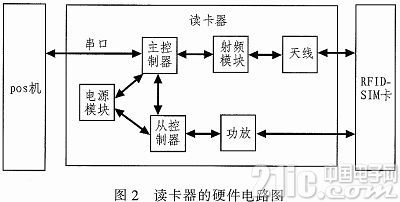
2.1 Power Module
In the card reader, the power module controls the power supply mode of the card reader in addition to powering the various modules inside the card reader. After inputting +5 V through DC or via USB, the 3.3 V input voltage is generated by the level shifting chip (MAX1818) to other modules.
2.2 main control module
The main control module is the core part of the card reader. The data between the card reader and the POS machine is transmitted through it. It is mainly responsible for the initialization of the RF module, the distance control module and the collision prevention detection. This paper selects Z32H256UF chip of National Technology Co., Ltd. The main performance of this chip is: 1) Multiple communication interfaces, including USB interface, IS07816 main controller, UART interface, SPI interface, FLASH/RAM main interface, 27-channel GPIO Interface; 2) Built-in oscillator controller and PPL, can be connected to 4 ~ 12 MHz crystal; 3) can achieve on-chip key management, on-chip signature and identity verification; 4) support low power consumption, chip power consumption is less than 500 mV (5 V @96 M main frequency) and 300 mV (5 V@24 M main frequency).
2.3 RF Module
This article uses Nordic's nRF24L01 chip to implement RF signal transmission and reception. nRF24IjD1 is a GFSK single-chip RF transceiver chip that operates in the 2.4-2.5 GHz ISM band. The chip includes: a frequency generator, a power amplifier, an enhanced SchockBurstTM mode controller, a crystal oscillator, a modulator, and a demodulator. The main features are: 1) Using the global open 2.4 GHz frequency band, with 80 optional working channels, short channel switching time, meeting the needs of multi-frequency communication and frequency hopping, the RF channel is set to 2.4 G by default, and the bandwidth is set to 1. MHz. 2) The wireless rate can be selected from 1 Mbps or 2 Mbps through the configuration register. 3) Working in the enhanced SchockBurstTM mode with automatic response and automatic retransmission, reducing the workload of the master MCU (Z32). That is: after the data transmission is completed, the chip immediately enters the receiving mode, waits for the response signal of the other party, and if not received, returns to the transmission mode to resend the data until a correct response is received or the retransmission exceeds the maximum number of times. 4) Low-power applications: When operating in transmit mode, the current consumption is 9 mA at a transmit power of -6 dBm and 12.3 mA in receive mode; the current consumption is lower in power-down mode and standby mode. 5) Built-in functions such as CRC check, packet identification, carrier detection, and few peripheral components. 6) Negotiate the communication address and frequency during data communication to ensure the correct and stable transmission of the signal. 7) Operating parameters such as operating frequency, transmit power, channel address, and data communication rate can be achieved through software settings.
2.4 low frequency module
The low frequency module is mainly composed of C8051F330 chip, amplifier and low frequency coil, and is mainly responsible for the generation, amplification and transmission of low frequency signals. The C8051F330 is available in a 20-pin MLP package with on-chip power-on reset, clock oscillator, VDD monitor, 10-bit current output DAC, 25 MHz internal oscillator, 768-byte on-chip RAM, full-duplex UART, SPI port, 128-byte special function registers, 17 I/O ports, 8KB of FLASH memory that can be programmed in the system, 8KB of which can be used in system-programmed FLASH memory for non-volatile data storage, allowing field-updated 8051 firmware. User software has full control over all peripherals and can shut down any or all of the peripherals to save power.
3 Conclusion
The White Paper on China's Online Payment Security issued by the Financial Research Institute of the Development Research Center of the State Council predicts that mobile payments will show explosive growth. It is expected that by 2017, the transaction scale of China's mobile payment market will exceed 2 trillion yuan. The growth rate will exceed 50% in the next few years. The card reader designed in this paper can support the mobile payment function of most mobile phones on the market. The card reader is designed as the master-slave module, the main controller module performs serial communication, and the controller module mainly accepts the main control. The device command realizes the control of the card swipe example and has broad application prospects.
Best Solar Flood Lights,Solar Motion Flood Lights,Solar Sensor Security Light,Commercial Solar Flood Lights
Jiangmen Liangtu Photoelectric Technology Co., Ltd. , https://www.liangtulight.com