In this issue, the author would like to discuss a topic that is both familiar and somewhat mysterious for analog engineers—Electrostatic Discharge (ESD), also known as "static protection." From the perspective of analog circuits, ESD is an essential yet often overlooked aspect of design.
According to Wikipedia, Electrostatic Discharge (ESD) is the sudden flow of electricity between two electrically charged objects caused by contact. In simpler terms, it's the instantaneous current generated when two objects with stored charges come into contact.
Recently, in my project, the ESD requirements have become much stricter. I've been discussing this with a colleague from the ESD department. He mentioned that ESD can occur anywhere—during manufacturing, production, assembly, testing, or even during transportation and field applications. At one point, I thought about giving up on dealing with it... but obviously, that’s not an option.
So the question arises: how do we simulate ESD in a circuit? Typically, we use two common models in circuit simulation: CDM (Charge Device Model) and HBM (Human Body Model).
CDM refers to the Charge Device Model, while HBM stands for the Human Body Model. These models represent different ways ESD can occur and must be accounted for in simulations.
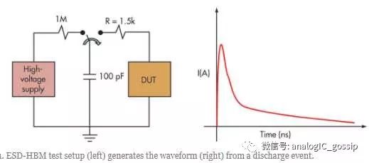
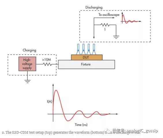
From the comparison, it's clear that the current from CDM is generally larger and faster than that from HBM because there's no significant resistance limiting the discharge path in CDM.
Therefore, in ESD simulations, we need to apply specific pulse voltages. For example, in a CDM scenario, a pulse of up to 15V with rise and fall times of 200ps over 4ns is required. In contrast, for HBM, the peak voltage is only 6V, with rise and fall times of 2ns and a duration of 400ns.
My colleague once said, “We are calculating the relevant value of this secondary ESD for you.†After all, it was a matter of deep digging and hidden knowledge... (I won’t tell you everything, just enough to make you curious.)
But why do we even consider secondary ESD protection? If there's a secondary, where is the primary?
We’re all familiar with the IO structure, particularly the pads with diodes above and below them. These diodes serve as the primary ESD protection.
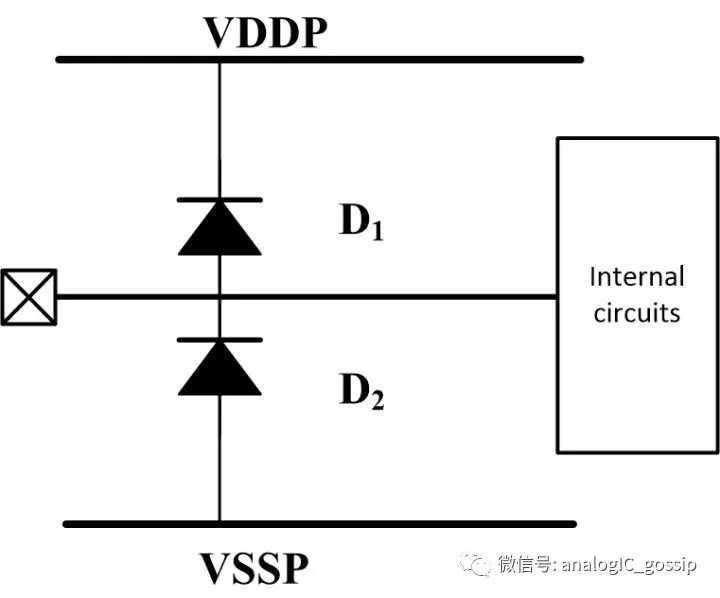
Universal IO with ESD protection
For example, under the HBM model, if +2000V is applied to the IO, the diode D1 turns on, directing the high voltage through VDDP. Similarly, if -2000V is applied, D2 turns on, allowing the current to flow from VSSP to the IO, preventing damage to internal circuits.
Now, here’s a question for everyone: VDDP and VSSP are the bias supplies for the IO diodes. So what exactly are the IOs of VDDP and VSSP? Can we place diodes on top of each other?
Think fast...
Of course not! I feel like that wouldn't work at all.
If there are no upper and lower diodes, how can we protect the IOs of VDDP and VSSP?
Let’s take a look at the actual IO circuits of VDDP and VSSP!
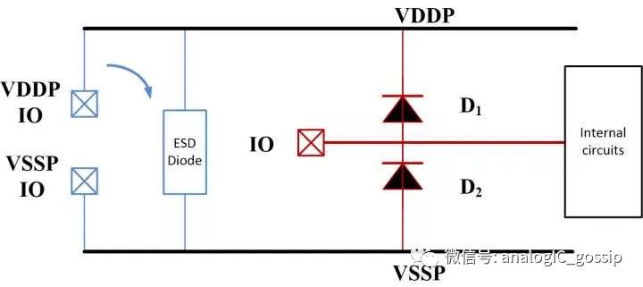
Including the IO ESD protection pad model
Therefore, additional ESD protection circuits must exist between the IOs of VDDP and VSSP. For instance, when VDDP is subjected to +2000V, the high-voltage current is quickly directed through the ESD diode. But what happens when VDDP is 0 and VSSP is at +2000V?
Wait, let’s think first. Are there two diodes in opposite directions?
...
After a moment.
If VSSP is at +2000V, does that mean all the IOs are going to be very active?
Why do you say that?
Well, all n-wells are biased to 0V by VDDP. If VSSP becomes 2000V, then aren’t all the parasitic diodes between the n-well and substrate turned on?
Wow! That sounds like a chaotic scene!
Then, I heard about the so-called “1 Ohm†principle. It states that the on-resistance from the IO to the ESD diodes must be less than 1 Ohm to avoid excessive parasitic resistance that could hinder rapid discharge. This helps prevent any “slipping fish†from entering the internal circuit. If you look closely at the IO layout, you’ll see that the metal layers are densely packed—literally “all the best.â€
Finally, let’s talk a bit more about the circuit (too lazy to draw, so I’ll borrow from somewhere):
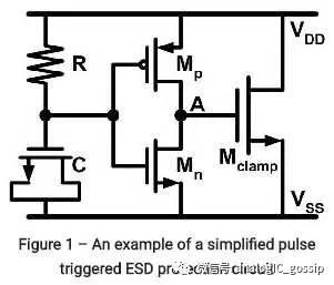
This is another type of ESD protection circuit. Why mention it? Because yesterday, I was asked to add an NMOS switch to my internal circuit. The gate of the NMOS is connected to point A in the figure. I was told that this is also part of the secondary ESD protection. (Note: This figure shows part of the IO, and the large NMOS Mclamp isn't part of the internal circuit. Here, the internal circuit is controlled via the IO’s internal nodes.)
Brief analysis: If a high voltage pulse appears on VDD, the capacitor doesn't immediately follow due to its voltage hysteresis. As a result, the gate voltage of Mp is much lower than the source, causing Mp to turn on. Point A then connects to VDD. The large Mclamp turns on, connecting VDD and VSS, thus diverting the high voltage away from the fragile internal circuits.
Back to the situation where I was asked to add a switch. The NMOS switch is similar to a power-down function but is controlled by point A. During a severe ESD event, the internal circuit can be shut down quickly, ensuring that the high ESD current doesn’t reach it.
Finally, I recommend a doctoral thesis: [http://ShuqingCao.pdf](http://ShuqingCao.pdf)
In this paper, it's explained in detail how the ESD Design Window is shrinking as process nodes get smaller. The gate oxide size is decreasing, leading to a lower breakdown voltage and a narrower range for ESD protection. It's quite a tough challenge!
From the author's comparison, the IOs of 0.18um and 28nm don’t look too different (though 28nm seems a bit bigger). We’ve spent so much effort reducing the process size, but the IO area remains a bottleneck. It's a sad story indeed!
One final note: ESD often requires a trade-off between performance and leakage. If the ESD diode is too large, the protection is better, but the leakage increases, affecting normal operation. Always weigh the pros and cons when using ESD protection.
Doorbell transformers are typically installed at the point where the doorbell system connects to the main electrical supply. They are compact, lightweight, and designed for easy installation and maintenance. These transformers are widely used in residential, commercial, and industrial settings, where doorbells are an essential part of security and communication systems.
Key Functions
Voltage Conversion:
The primary function of a doorbell transformer is to step down the voltage from the standard household AC supply (e.g., 110V or 220V) to a lower DC or AC voltage required by the doorbell system. Common output voltages include 12V DC, 16V DC, or 10V AC.
Safety:
By converting high voltage to low voltage, doorbell transformers provide a layer of safety, reducing the risk of electrical shock or fire hazards associated with high-voltage circuits.
Compatibility:
Doorbell transformers are available in various specifications to accommodate different types of doorbell systems, including wired, wireless, and smart doorbells. This ensures compatibility with a wide range of doorbells and installation environments.
Technical Specifications
Input Voltage: The voltage range at which the transformer can accept power from the main supply.
Output Voltage: The voltage level at which the transformer supplies power to the doorbell system.
Output Current: The maximum current the transformer can deliver at the specified output voltage.
Power Rating: The total power the transformer can handle without overheating or damaging the circuit.
Size and Weight: Physical dimensions and weight, which can affect installation requirements and space constraints.
Connector Type: The type of output connector used to connect the transformer to the doorbell system (e.g., screw terminals, push-in connectors).
Installation and Maintenance
Installation: Doorbell transformers are typically installed near the electrical panel or in a convenient location close to the doorbell system. They require basic electrical wiring knowledge and follow standard electrical codes and regulations.
Maintenance: Regular maintenance involves checking the voltage output and wiring connections to ensure the transformer is functioning properly. Replacement may be necessary if the transformer fails or the doorbell system requires an upgrade.
Smart Home Integration
With the rise of smart homes, some modern doorbell systems are designed to integrate with other smart devices and home automation systems. While these systems may not require a traditional doorbell transformer due to built-in power management modules, they still rely on power conversion principles similar to those employed by traditional doorbell transformers.
Conclusion
In summary, doorbell transformers are essential components of doorbell systems, providing safe and reliable power conversion from standard household AC supplies to the lower voltages required by doorbells. Their technical specifications, ease of installation and maintenance, and compatibility with various doorbell types make them indispensable in residential, commercial, and industrial settings. As smart home technology continues to evolve, doorbell transformers may evolve alongside these systems, adapting to new power management requirements and integration capabilities.
Doorbell Transformer,nest doorbell transformer,24v doorbell transformer,buck boost transformer
Guang Er Zhong(Zhaoqing)Electronics Co., Ltd , https://www.geztransformer.com