In this issue, the author would like to discuss a topic that is both familiar and somewhat mysterious for analog engineers—Electrostatic Discharge (ESD), also known as "static protection." From an analog circuit perspective, ESD is a critical concern that can cause serious damage if not properly managed.
According to Wikipedia, Electrostatic Discharge (ESD) refers to the sudden flow of electricity between two electrically charged objects caused by contact. In simpler terms, it’s the instantaneous current that occurs when two objects with stored charges come into contact.
Recently, in my project, the ESD requirements have become more stringent, and I often find myself discussing this with a colleague from the ESD department. He mentioned that ESD can occur anywhere—during manufacturing, production, assembly, testing, even during transportation or field use. At one point, I thought about giving up on handling it entirely... but obviously, that’s not an option.
So, the question is: how do we simulate ESD in a circuit? Generally, there are two main models used in circuit simulation: CDM (Charge Device Model) and HBM (Human Body Model). These models help us replicate real-world ESD events and test the robustness of our designs.
CDM represents the discharge that happens when a charged device comes into contact with a grounded object. HBM, on the other hand, simulates the discharge caused by a human body touching a device. The key difference is that CDM typically produces a much higher and faster current because there's no significant resistance limiting the discharge path.
To simulate ESD in a circuit, we need to apply specific pulse voltages. For example, in a CDM scenario, the voltage might be a 15V pulse with rising and falling edges as fast as 200ps, lasting for 4ns. In contrast, the HBM model usually involves a 6V pulse with slower edges (2ns) and a longer duration of 400ns.
Here’s a quote from my colleague: “We are calculating the relevant value of this secondary ESD for you.†After all, it’s a matter of deep digging and careful analysis. (Don’t worry, I won’t tell you how to count—it’s complicated.)
But why do we even talk about secondary ESD protection? If there’s a secondary, where is the primary? We’re all familiar with the IO structure, which includes diodes above and below the pad—these are the primary ESD protection mechanisms.
For example, in an HBM model, if +2000V is applied to the IO, the diode D1 turns on, directing the high voltage through VDDP. Similarly, if -2000V is applied, D2 turns on, allowing the current to flow from VSSP to the IO, protecting the internal circuitry.
Now, here’s a question: VDDP and VSSP are bias supplies for the IO diodes. What exactly are the IOs connected to VDDP and VSSP? Can we just stack diodes on top of each other?
No, of course not! That wouldn’t work. So, how do we protect the IOs connected to VDDP and VSSP? There must be additional ESD protection circuits between them.
Take a look at the IO circuits of VDDP and VSSP. There should be ESD diodes in place to quickly channel any high-voltage surges. For instance, if VDDP is subjected to +2000V, the ESD diode directs the current away. But what if VSSP is at +2000V instead?
This is where things get tricky. Are there two diodes in opposite directions to handle both positive and negative voltages? Yes, that’s the idea. But what if VSSP is at a high voltage? Then, all the parasitic diodes between nwell and substrate might turn on, creating a dangerous situation.
That’s why there’s a so-called “1 Ohm†rule. The on-resistance from the IO to the ESD diodes must be less than 1 Ohm to ensure fast discharge and prevent unwanted currents from entering the internal circuit. This is why the layout around the IO is so dense—every metal line is carefully placed to minimize resistance.
Finally, let me mention another ESD protection circuit. It’s a bit complex, but I’ll keep it simple. Here’s a diagram:
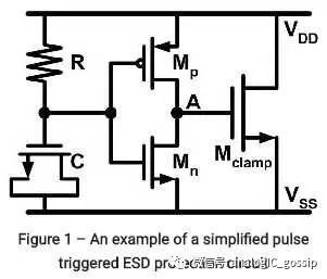
This circuit includes a capacitor and a PMOS transistor. When a high voltage pulse appears on VDD, the capacitor doesn’t charge immediately due to its hysteresis. As a result, the gate of the PMOS is lower than the source, turning it on. This connects point A to VDD, triggering the large Mclamp transistor, which then shorts VDD to VSS, protecting the internal circuit.
I was recently asked to add an NMOS switch to my internal circuit, controlled by point A. This is part of the secondary ESD protection. The NMOS acts like a power-down switch, turning off the internal circuit during a severe ESD event to prevent damage.
To wrap up, I recommend reading a doctoral thesis titled *“ESD Design Window Shrinking with Process Scalingâ€* (available at [http://ShuqingCao.pdf](http://ShuqingCao.pdf)). It explains how ESD design becomes more challenging as processes scale down. Smaller gate oxides mean lower breakdown voltages, making it harder to protect circuits effectively.
Interestingly, even though 28nm technology is much smaller than 0.18um, the IO structures don’t look that different. This highlights a major challenge in semiconductor design: shrinking the process while maintaining ESD protection capabilities.
Lastly, ESD protection always involves trade-offs. Larger ESD diodes provide better protection but increase leakage current, which can affect normal operation. It’s all about finding the right balance.
USB Charger refers to a device designed to provide power and charge electronic devices through a USB interface. It typically plugs into an AC outlet or another USB port and delivers electrical energy to connected devices via a USB cable.
Main Types
Standard USB Chargers: Plug directly into AC outlets and charge devices through USB ports.
Car USB Chargers: Mounted in a vehicle's cigarette lighter socket, providing charging capabilities for in-car electronic devices.
Quick Charge USB Chargers: Support fast charging technologies like Quick Charge (QC) or Power Delivery (PD), enabling devices to charge more rapidly.
Market Landscape and Trends
Current Market Status: With the proliferation of electronic devices and advancements in fast charging technology, the demand for USB Chargers continues to grow. Consumers have a wide range of brands, models, and features to choose from.
Future Trends: USB Chargers are evolving to prioritize charging efficiency, safety, and portability. Fast charging technologies will see wider adoption, while the development of wireless charging may lead to the emergence of wireless USB Charging solutions as a new market trend.
Usb Charger,Usb Charger Adapter,Usb Charger Adapter Plug,Usb Port Travel Adapter
Guang Er Zhong(Zhaoqing)Electronics Co., Ltd , https://www.geztransformer.com