1 Introduction
Today, LEDs are widely used in LCD backlights, automobiles, traffic lights, and general lighting. According to IEC 61000-3-2 Class C regulations, Power Factor Correction (PFC) is required for LED general-purpose illumination drivers larger than 25W, so low-cost power factor correction schemes have become a research topic of interest.
The Active Power Factor Correction (APFC) circuit commonly used in AC/DC converters is a two-stage PFC circuit. The first stage circuit is used for power factor correction, and the latter stage circuit is used as a DC/DC converter. Since there are two cascaded power stages, the size and cost of this type of circuit are usually high. Therefore, another type of APFC topology emerges. This type of topology integrates the PFC circuit and the DC/DC converter, and they share An active power switch becomes a single-stage AC/DC converter, which reduces the cost. This APFC circuit is now widely used in ballasts and chargers.
Using a multi-output converter as an LED driver enables a converter to meet multiple different levels of constant current output requirements, thereby reducing the cost of the driver. The traditional multi-output converter, such as transformer coupling mode and weighted feedback adjustment mode, can realize multi-channel constant voltage output, but cannot realize multi-channel constant current output. Based on this, this paper proposes a class of dual-output single-stage flyback PFC topology.
Under the DCM, this kind of topology can realize independent voltage regulation of independent regulation, and can realize independent constant current output of each channel, and realize power factor correction. In order to avoid the cross-effect of the two outputs of the converter, the time division multiplexing method is used to realize the independent adjustment of each output branch current, so that each channel can drive different types of LEDs separately, and one of the drivers will not affect the other. The normal output of the branch improves the reliability of the driver; since only one magnetic component is used in this method, two constant current outputs can be realized, and a large high-voltage storage capacitor is not required after the rectifier bridge, thereby reducing the cost of the driver. The converter operates at DCM, fixed frequency, and fixed duty cycle, and can also achieve higher power factor. Finally, the correctness and effectiveness of the research results are verified by simulation and experiment.
2 Independently adjust the double constant current output flyback topology
Figure 1 shows the topology of the single-stage flyback PFC converter with independent regulation of dual constant current output and its switching timing. Figure 1 (a) shows the independent output winding topology, with the two outputs being provided by two separate windings.
Figure 1(b) shows the shared output winding topology. The two outputs are provided by the same winding time division. Regardless of the independent output winding type or the common winding type, if the two circuits satisfy D1a + D2a < 0.5, and D1b + D2b < 0.5, the two paths can be operated in complementary phases Фa and Фb, by time division. The two channels are multiplexed and controlled by Signal TMS (Time-Multiplexing Signal, TMS). As shown in Figure 1 (c), when Soa = 1, the converter adjusts the output of the A, the primary switching current Ip rises linearly in the D1aT phase, and the current Isb decreases linearly in the D2a T freewheeling phase, D3a T = ( 1 - D1a - D2a) T, the current Isb is zero, at this time, the converter is in DCM mode; when Sob = 1, the converter adjusts the B output, and if the B is working, the converter is also in DCM mode. It can realize two-way cross-influence control.
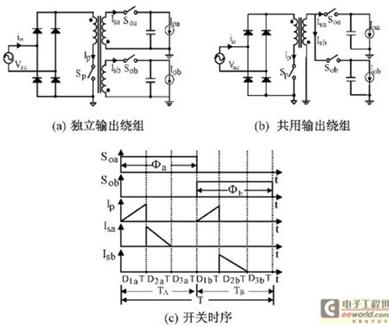
Figure 1 Independently regulated dual output single stage flyback PFC converter and its switching timing
The Flyback converter has native PFC capability in DCM mode, and the input current automatically tracks the input voltage while maintaining small current distortion. If the converter operates at DCM, fixed frequency, and fixed duty cycle, the converter can achieve a higher power factor. For the dual output flyback converter proposed in this paper, if the DCM mode has no cross-effect, if the high power factor can be realized in each way, the whole converter can also achieve a higher power factor.
3 power factor correction control implementation
Figure 2 shows a voltage-mode PWM control dual-output single-stage flyback PFC LED driver and control implementation. Each channel is connected by LED in series. The sampling voltages Voa and Vob of the two output currents of A and B are respectively compared with two reference voltages Vref1 and Vref2, and then the error signals Ve1 and Ve2 are generated by the error comparator. The sawtooth wave signal Vsaw is simultaneously compared with the two error signals. Generate C1, C2 signals.
The time division multiplexed signal TMS generated by the time division multiplexed signal generator provides a selection signal to the selector, thereby determining that the controller selects each duty cycle signal C1 or C2 in one cycle. The output signal Vs1 of the selector is isolated. As the drive signal of the main switch Q1, the time division multiplexed signal Vsa (TMS) and its complementary signal Vsb serve as drive signals for the switches Q2 and Q3, respectively.
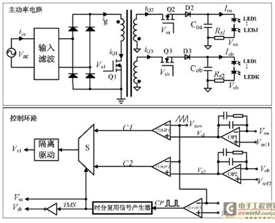
Figure 2 Schematic diagram of dual output single-stage flyback PFC driver and control loop
Figure 3 shows the control timing diagram of the primary-side current iQ1 and the secondary currents iQ2 and iQ3 of the dual-output single-stage flyback PFC converter. The time division multiplexed signal (TMS) determines the branch of the regulation. When TMS = 1, the converter adjusts the A path. At this time, the converter works according to the design parameters of the A circuit. The peak envelope of the primary and secondary switching currents of this path are respectively IQ1_A( θ) in Figure 3. And Ipkp_Q2( θ); when TMS = 0, the converter adjusts the B path. At this time, the converter works according to the design parameters of the B path. The primary and secondary switching current peak envelopes of the path are respectively As shown in Figure 3, IQ1_B( θ) and Ipkp_Q3( θ); The average input current of the converter is the average of the two input currents, as shown by IQ1_avg( θ) in Figure 3.
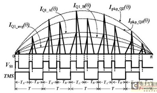
Figure 3 Schematic diagram of control timing of dual output single-stage flyback PFC converter
In order to achieve constant duty cycle control, the bandwidth of the single-stage flyback PFC converter error amplifier must be less than 2 times the power frequency, generally about 10~20Hz, so the error amplification network is set to output the power frequency ripple and the input sinusoidal voltage. It is not very sensitive, and the duty cycle requirement can be realized to realize PFC.
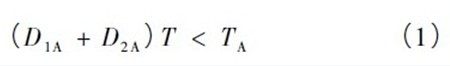
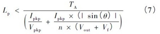
In order to make the dual outputs have no crossover effects and PFC functions, it is very important to ensure that the circuit works under DCM. In order to ensure that the inductor current is in discontinuous mode, the A path should satisfy:
After the input voltage is rectified by the full bridge, it can be expressed as:
Where Vpkp is the peak value of the input voltage, θ is the input frequency, T is the switching period (= TA + TB), and TA is the multiplexing time of the A channel in one switching cycle. In the half-frequency cycle, the converter's envelope of the input current peak value is at the fixed duty ratio:

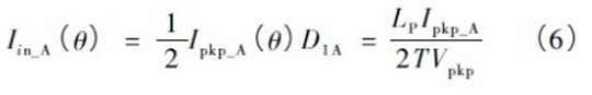
Ipkp_A is the maximum peak value of the input current of the A channel. The on-time of the main switch of channel A is:

Among them, LP is the primary inductance value. The turn-on time of the secondary side switch of A is:
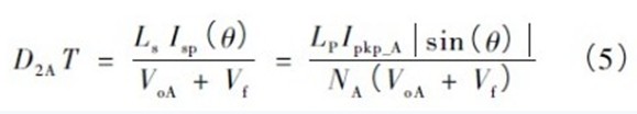
Where LS is the secondary side inductance value; ISP(θ) is the secondary current peak value, which is also a sinusoidal function; NA is the primary side and the secondary side turns ratio; Vf is the secondary side diode conduction voltage drop.
The instantaneous input current of channel A is:
To ensure that the A-way works in the discontinuous mode, it is necessary to satisfy the formula (1) and substitute the equations (4) and (5) to obtain the critical inductance:
The average power of the A input can be expressed as:
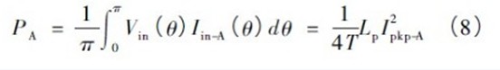
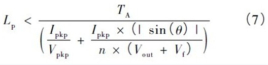
If Lp is fixed, the maximum peak value of the primary circuit switching current of channel A is:

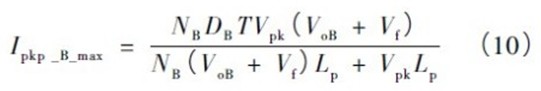
Similarly, the maximum peak value of the primary peak current of the B channel is:
If the converter has no energy loss, the maximum output power of the A and B channels is:
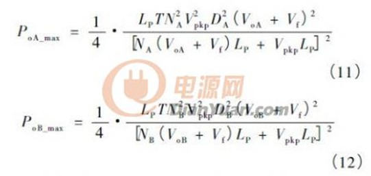
If the two output voltages are equal, according to equations (11) and (12), then the relationship between the maximum output power of channel A and channel B and the duty cycle DA of channel A is shown in Figure 4:
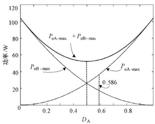
Figure 4 A and B road maximum output power and DA
It can be seen from Fig. 4 that if the required power of the two channels is different, such as PA /PB = 2, DA selects 0. 586 to maximize the total output of the converter output while satisfying the two output powers. Critical conduction mode. Therefore, the multiplexing time can be allocated according to the maximum demand power of each channel, which can improve the utilization of the inductor.
4 Simulation and experimental results
In order to verify the feasibility of the dual output single-stage flyback PFC converter, according to the independent regulated dual output flyback converter and control implementation requirements shown in Figure 2, the circuit parameters of Table 1 were selected for simulation and a prototype was fabricated. In order to simplify the design, the ratio of the primary side to the secondary side of the transformer is set to 36:9:9, and the multiplexing time ratio of the time division multiplexed signal is selected as TA: TB = 1:1, as shown in Table 1.