Today, FPGAs are powerful and have a large number of pins, giving engineers plenty of opportunities to enhance features and functionality while reducing product costs. As complexity increases, integrating these devices into printed circuit boards is also a serious challenge. Hundreds of logic signals need to be mapped to the physical pinout of the device while maintaining the electrical integrity of the design. The increased complexity of FPGAs also requires advanced synthesis techniques to achieve timing closure faster, minimizing the impact of design changes and addressing specific application requirements.
These challenges can be addressed by using optional FPGA-PCB optimization techniques that add HDL synthesis and advanced FPGA-PCB I/O optimization to PADS Professional. This interface between the HDL design environment and the physical implementation on the PCB significantly reduces time-to-market and lowers manufacturing costs.
Intuitive logic synthesis environments include advanced optimization techniques, award-winning timing analysis, and advanced inference techniques for vendor-independent designs that accelerate time-to-market, eliminate design flaws, and provide superior results quality ( QoR).
FPGA I/O optimizes pin assignments for improved routing and signal integrity.
Main advantages:
â– Reduce total design time by using parallel processes â– Reduce PCB manufacturing costs by eliminating PCB signal layers â– Eliminate PCB redesign due to outdated FPGA symbols on PCB â– Optimize with high speed performance â– Eliminate and create and maintain schematics for PCBs FPGA symbol related costs
FPGA I/O OpTImizaTIon
Process integration
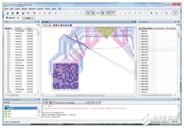
I/O optimization is tightly integrated with the PADS Professional design process and is accessible at any stage of the project. The schematic, PCB Layout, and FPGA database are always in sync so that the user can control the design data flow of the project. In addition, the schematic user can decide when to transfer FPGA data (new or updated data) to the PCB design.
I/O optimization can use PADS project data for stack planning and optimization of initial allocation before PCB layout or routing begins. Users can export results to a Layout and manage FPGA components at the project level or at the enterprise library level.
Signal and Pin Assignment Manually assign hundreds of HDL signals to the FPGA pins while still adhering to the FPGA vendor rules, which can be difficult. To streamline this process, PADS Professional provides easy-to-use features for automatic assignment, signal standard supervision, simple drag-and-drop assignment, support for operands, and dynamic filtering. In summary, it simplifies the signal pin assignment operation flow. Each pin assignment change is managed through the FPGA-PCB process and is consistent regardless of where it is changed.

Automation components and symbol generation require different symbol generation process methods due to the nature of the FPGA device itself. During the life of the project, the FPGA logic is usually changed several times, and the symbols must be consistent with these changes. This advanced PADS module is powerful, not only allows you to create symbols easily, quickly and without errors, but still has full control over the symbol creation process. Time is reduced from hours or days to minutes compared to manual symbol creation.
Laminated planning
An important stage in the PCB design flow is the component layout and its orientation on the PCB layout. You can plan stacking before or during the PCB Layout process. As a result, engineers and designers have the distinct advantage of making FPGA pin assignment changes, optimizing component placement and orientation, shortening flying leads, and reducing flying line interaction during the initial stages of the project.
FPGA Multiple Instances and Optimizations In most cases, the same FPGA device has different logic functions in different projects and even in one project. PADS Professional I/O Optimization automatically supports these conditions during project development. The FPGA and vendor component numbers for different functional symbol representations are listed in the bill of materials report. Basically, it is not possible to successfully perform connection optimization between two or more FPGA devices manually. But with this advanced PADS Professional module, the optimization algorithm can evaluate all possible combinations of connections for the best interconnection. In addition, the network interaction generated in the initial allocation can be minimized and the wiring completion rate can be improved.
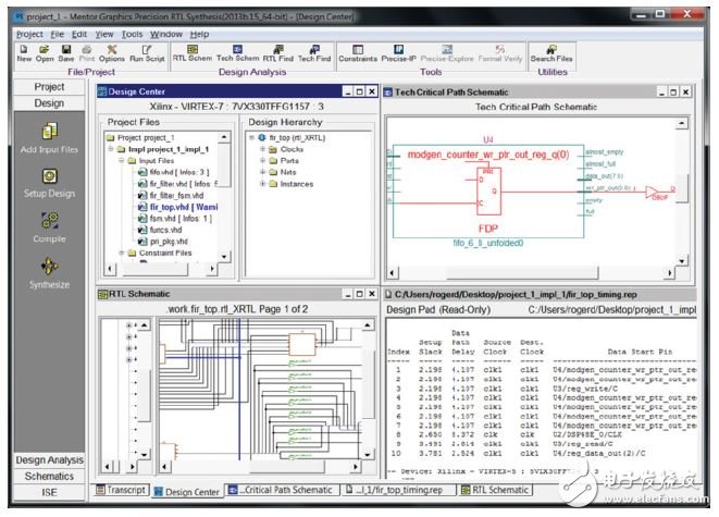
FPGA Synthesis
Advanced Optimization Algorithms A unique set of optimization algorithms automatically focus specific optimizations on design areas that are most likely to hamper overall performance, such as finite state machines (FSMs), cross-hierarchical paths, and paths with excessively high combinational logic. These algorithms provide automated heuristics to deliver smaller and faster designs without the need for iterative human intervention.
When the RTL and the Technology Schematic Viewer are compiled, they can be created using a generic gate and viewed in an RTL schematic. After synthesis, the technology map database is created using the technical schematic that reflects the database. The schematic viewer helps you understand how to interpret RTL and map it to target FPGA technology.
Supplier irrelevance vendor-independent synthesis support for Altera, LatTIce, Microsemi and Xilinx devices. Therefore, you can use the same HDL design source files and constraints to target any device and get a synthetic netlist for placement and routing with the appropriate vendor tools. This vendor irrelevance makes it easy for users to retarget any FPGA device and analyze the results to find the FPGA device that best fits your design.
Use advanced synthesis techniques in a vendor-independent environment to achieve specific architectural optimizations for each FPGA device.
Support for all devices In addition to supporting FPGA devices from the four major FPGA vendors, the PADS FPGA-PCB Collaborative Design Module fully supports Altera Quartus II, LatTIce Diamond and ispLEVER, Microsemi Libero and Designer, and FPGA vendor tools such as Xilinx ISE and Vivado.
Simplifying the Constraint Process To accommodate today's highly complex FPGA design flows, you need to support a variety of constraint sources, including specific constraint sources such as HDL code, SDC files, and global constraint sets in tools. Be sure to specify common timing constraints such as clock frequency, input/output delay, and timing anomalies (eg, multi-cycle and pseudo-path in synthesis) to ensure optimal results from synthesis.
Gated clock conversion
ASIC designers typically use gated clocks for power management and other operations. However, when mapped to an FPGA, these gated clocks can cause large clock skew, create spurious signals, and hinder timing analysis. The gated clock is automatically converted using the appropriate enable signal in the FPGA.
DSP and RAM Inference Optimization Today's advanced FPGA devices include DSP and RAM embedded modules in addition to conventional logic blocks. In this way, the synthesis tool understands the various RTL coding styles and maps them to the appropriate DSP or RAM blocks to take advantage of resources and get the best performance. The PADS Professional FPGA-PCB Collaborative Design Module features advanced inference and optimization capabilities to maximize the use of embedded resources to increase area utilization and frequency.
Verilog, SystemVerilog, and VHDL support By using industry-leading language support such as Verilog, SystemVerilog, and VHDL/VHDL-2008, designers can create and synthesize RTL designs in any combination of these formats for optimal results.
Description of self closing Wrap Around Cable Sleeve Wire Harness
PET White Self Wrapping Split Braided Sleeving for cable management (PET woven mesh tube) is braided by environment friendly polyester monofil. PET is with good flexibility, fire resistance, abrasive resistance and thermal insulation performance. The sleeving are smooth surface, bright color, various patterns.
self-closing wrap offers innovative solutions for the protection of breakout areas and provides easy removal when is necessary an inspection or maintenance of cables. The special open structure allows to be installed after other components, for example copper terminals and connectors.
flexible semi-rigid wrappable split PET braided cable sleeving is a perfect solution to protect wires, cables, wire harnesses where ease of installation is paramount. With a 50% overlap, this sleeving wraps securely to itself eliminating the need to secure the sleeving opening with any other method.
Self closing wrap is a non-expandable sleeve woven from monofilament weft and multi-filament warp.
It provides a lightweight, cost effective and tough solution for protection of a wide range of wire and cable.
Its inherent flexibility allows it to be bend, coil and fit with irregular shapes while its open design allows it to be install on finished assemblies quickly.
Wrap Around Cable Sleeve,Sleeve For Wires ,Self Cable Wrap,Self Split Wrap
Shenzhen Huiyunhai Tech.Co.,Ltd , https://www.hyhbraidedsleeve.com