Abstract: In order to facilitate the scientific researcher to evaluate and test the new image processing algorithm in the design process of TV image processing system, reduce the design complexity of the evaluation test board hardware circuit, propose a solution here, and realize the PCI bus based. The design of the TV image real-time simulation system. The system firstly collects, pre-processes and video A/D conversion of the TV image through the PCI card, and then selects the digital image information with high-speed characteristics to write the digitized digital image information into the computer system memory, and finally on the computer terminal. Using high-level language programming, image processing and control interface software development, computer software access to PCI hardware devices, real-time processing, segmentation, matching and other algorithm simulation of digital images.
Keywords: PCI bus; TV image; real-time processing; digital image
0 Introduction With the improvement of the performance of TV image processing systems, designers need to constantly adopt new digital image processing algorithms. How to evaluate these new algorithms, how to transform theoretical design into engineering applications has become the primary concern of designers.
To realize TV image signal processing, it is necessary to design a complex circuit system, and the design of the hardware circuit should consider the development of high-speed DSP chip, ultra-large-scale integrated circuit design, video conversion, interface and other complex circuits. Designing printed circuit boards and debugging will take up more work time for designers. Longer development cycles and higher development costs are not conducive to the new ideas of image processing and the transformation of new algorithms into engineering applications. The simulation system can greatly reduce the complexity of the hardware circuit design and shorten the development cycle, which is conducive to the research and design personnel to concentrate on evaluating and testing the new algorithm.
The ability to acquire and process TV image signals in real time is a key issue in designing simulation systems. In view of the improvement of the computing speed of the microcomputer and the high-speed characteristics of the PCI bus, it is possible to design a real-time simulation system of the television image processing system based on the PCI bus. The system uses a microcomputer simulation television image processing system to process images, and uses a PCI card circuit to realize real-time collection and transmission of image data acquisition data. The development of PCI bus breaks the bottleneck of traditional microcomputer data transmission. The biggest disadvantage of traditional microcomputer bus is that the transmission rate is too low, real-time transmission of image data cannot be realized, and it cannot meet the requirements of image processing system and large-scale application. The PCI bus acts as a synchronous, processor-independent 32-bit local bus with a maximum operating frequency of 33 MHz and a peak data throughput of 132 Mb/s. Therefore, the time for transmitting one field (256 × 256 × 32 bits of data) by the PCI bus is not more than 20 ms. Due to the spatial and temporal redundancy of television signals, such as compression of signals, the time required to transmit a field of signal will be shorter. Therefore, in the simulation system, the data image information is directly transmitted to the system memory by using the PCI bus, and real-time transmission, storage, and processing of the data are possible.
1 Structure and function of the system Because the microcomputer is used as the data processing system, the workload of the hardware circuit design can be greatly reduced. The simulation system only needs to design a PCI card to realize timely collection and processing of image data. The principle block diagram of the system is shown in Figure 1. 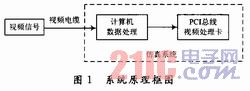
The PCI bus video processing card is used to preprocess the image and video A/D conversion, and then the digital image information is written into the computer system memory through the PCI bus, and the high-level language programming is used to realize digital image pre-processing, segmentation, target image processing, Matching algorithms.
2 PCI bus video signal processing card PCI bus video processing card consists of analog video signal processing, video signal A / D conversion, PCI bus data acquisition and signal transmission.
2.1 Video processing and video A/D conversion The video signal has a certain attenuation after transmission through the cable and adds a noise signal to amplify and filter the original video signal before A/D conversion, which can effectively enhance the video information. Reduce noise interference. There are many types of video A/D conversion chips available, such as SAA7111 and BT218.
2.2 PCI bus data acquisition and signal transmission PCI bus is burst transmission of group data, each group of data is composed of an address signal and a series of data signals, PCI bus uses address and data multiplexing structure, greatly reducing The number of signals, but the PCI bus specification is still very complicated. The implementation of the interface is more difficult than the traditional ISA and EISA bus. The devices connected to the PCI bus can be divided into two types: the main control device and the target device. The target device requires at least 47 signals. The master device requires a minimum of 49 signals, including data/address multiplexing bus, interface control lines, arbitration, bus commands, system lines, and so on. In the design, the following two solutions can be used to implement the interface design of the PCI bus:
2.2.1 PCI Interface Design Using Programmable Logic Devices Almost all programmable logic device manufacturers currently have typical PLD products for microcomputer interfaces. Most manufacturers also provide PCI bus interface core design modules compiled with VHDL, Verilog, and AHDL. A simple PCI bus interface design can be implemented using these modular programmable logic devices. Due to the characteristics of the programmable logic device itself, designers have more space for thinking and imagination when implementing PCI interface design.
Although the use of programmable logic devices to design PCI interfaces is flexible, there are still some issues to be concerned in the design:
(1) PCI is compliant. Almost all logic in high-performance data and control paths requires a copy of PCI system time, which is inconsistent with PCI's demanding load requirements. In addition, when performing certain functions such as data burst transfer, a lot of clock load is often required, and the clock rising edge to output valid time must be less than 11 ns, which further aggravates the clock fanout problem.
(2) The PCI specification imposes stringent 7 ns setup times for transmitted data, sometimes using analog delays in the design.
(3) Any perfect PCI interface device must provide PCI configuration space. To implement PCI specified functions, complete the basic requirements such as logic check, address decoding, and various types of registers required for configuration. Select programmable devices for their logic. The capacity of the door has a large requirement.
In addition, when using the programmable logic device to design the plug-in circuit, it is necessary to add circuits such as FIFO, user register, and back-end device interface, which increases the difficulty of circuit design to some extent.
2.2.2 Select PCI chip controller dedicated chip Place a dedicated chip between the card circuit and the PCI bus to provide data and control signals. Such as PLX9080 and PLX9054 series chips developed by PLX, AMCC's S59xx series, etc. AMCC's S5933 is a powerful and flexible PCI bus controller interface chip. It is available in 160PQFP and 208TQFP packages. It conforms to the PCI local bus specification and can be used as a PCI bus target device (Slave) for basic transmission. It can also be used as a PCI bus master (Master) to access other bus devices. The principle block diagram is shown in Figure 2. 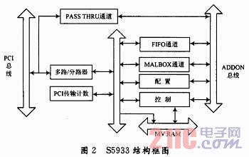
S5933 provides three physical bus interfaces: PCI bus interface, ADD-ON bus interface and external configuration memory (BIOS-ROM) interface. Data transmission can be performed between PCI bus and ADD-ON bus or with external configuration memory. The transmission between the PCI bus and the ADD-ON bus can use three channels: a mailbox register channel, a FIFO channel, and a PASS-THRU channel.
(1) Mailbox register channel. S5933's mailbox register (MAILBOXES) provides a bidirectional data path, mainly used to transfer command and status information between the multiplexer/splitter and the AD-DON bus, and can be based on the specified MAILBOX event, either on the PCI bus or ADD-ON bus. An interrupt is generated.
(2) FIFO channel. The FIFO channel mainly includes two 32×8 FIFOs for data transmission from PCI to ADD-ON and ADD-0N to PCI. Both FIFOs support PCI bus master operation and support burst transfers.
(3) PASS-THRU channel. The PASS-THRU transmission channel provides a registered access port for the PCI bus, and accesses resources on the ADD-ON through the handshake protocol. The PASS-THRU channel can only be used as a target device to support burst transmission.
Comparing the above two schemes for implementing the PCI interface, it can be seen that the programmable logic device can flexibly implement the required functions. For the PCI interface circuit design of this system, it is not necessary to implement all the functions in the PCI specification, and the programmable logic device can also provide a solution to the problem. However, in order to meet the stringent requirements of the PCI index, a large amount of logic verification and timing analysis work is required. The PCI dedicated chip such as the S5933 can be used to easily implement the PCI interface design, which greatly shortens the development cycle.
3 Computer Data Processing In order to implement the simulation function, it is also necessary to develop related image processing and control interface software. Drivers under Windows include hardware drivers for non-physical devices such as hardware drivers and file systems. Because the Windows operating system limits the access resources of the application in order to ensure the security, stability and portability of the system, it is necessary to develop the relevant device driver regardless of whether the programmable logic device or the dedicated interface chip is used to implement the PCI interface design. Program that implements computer software access to PCI hardware devices.
3.1 Device Driver Development There are several development tools available for developing device drivers. Mainly include: Microsoft's software package (device drtver K6t, ddK); Numega's VtoolsS; KRF-Tech's WinDriver.
Before developing device drivers, you must first analyze hardware device features, bus structure, interrupt settings, data transfer mechanisms, and device memory. The basic functions that the driver needs to perform include device initialization, read and write operations to the port, interrupt settings, responses and calls, and direct read and write to memory.
3.2 Simulation System Driver Development Image processing software is written using Microsoft's powerful VC++ high-level programming language. Open a space in the memory of the computer system, store the digital image information transmitted by the PCI bus and the feedback amount of the controlled system, use VC++ programming to realize the read and write operations of the computer memory, and realize the digital filtering and histogram of the image by the high-speed computing function of the computer. Image processing algorithms such as statistics, binarization processing, edge detection, target feature selection, etc., and display the acquired image, feedback amount, processed image, and feedback amount on a computer monitor, and the designer can directly obtain the image processing intermediate. Through various processes of image processing, designers can easily find the advantages and disadvantages of different image processing algorithms, and thus optimize and improve various image processing algorithms.
4 Conclusion The TV image simulation system designed by this method has been successfully applied in the development of infrared image recognition, processing and control of a weapon system. The system fully utilizes the high-speed characteristics of the PCI bus and the large degree of freedom of data processing of the microcomputer, and is flexible and reliable, effectively solving the problems of real-time collection, transmission, storage and real-time processing of the television image, and at the same time, the technical reserve for the designer. And the system's pre-design helps, and has a strong application value.
This article refers to the address: http://
LED Usb Cable advantage:
Hot selling colors gradual change color Led Usb Cable flashing data charging cable for ios ,for android,100% Brand New and High Quality.
Standard USB 2.0 Cable.Start syncing your phone with a PC today through this premium quality Data Cable.All the Cellphones with Micro USB Port

LED USB Cable
Led Usb Cable,Durable Usb Cable,Mini Usb Adapter Cable,Led Light Usb Charger Cable
Dongguan City Leya Electronic Technology Co. Ltd , http://www.dgleya.com