I. Preface
This is a technical article that is not very targeted. In this article, I studied and discussed the RF circuit design in Wi-Fi products, including various components, such as wireless transceivers, power amplifiers, and low-noise amplifiers. If you discuss a part of this article, you can Write a very thick book.
This article is general. Although this article mainly analyzes Atheros and Ralink's solutions, the solutions of these two vendors are very representative and have a high market share. Therefore, most Wi-Fi products must be consistent or A similar architecture. People who frequently browse related websites must know that wireless routers that are popular in the Chinese market, wireless APs are many of these two solutions.
This article has some practicality. This article is based on more than 20 reference design circuits of our company, fully absorbs the essence of the reference design, and extracts its generality. At the same time, this article also focuses on the analysis of the actual circuit structure and the selection of devices should pay attention to The problem has not been studied in depth, so this article has certain practicality.
This article was written by me in my spare time (also I can kill time in this way). If this article can bring a little help to everyone's work, it will be my happiest thing.
Chapter 1. RF Design Block Diagram
When you are technical and explain the principle of a design, you will start with a block diagram. I am no exception. Let me show you the general RF design block diagram of Wi-Fi products.
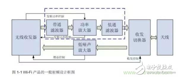
Figure 1-1 General RF design block diagram of Wi-Fi products
As shown in Figure 1-1, the RF part of a typical Wi-Fi product consists of five parts (this is my personal opinion, different engineers may have different ideas), and the blue dotted line is uniformly regarded as power. Amplifier section. Radio Transceiver (Radio Transceiver) is generally one of the core components of a design. In addition to its close relationship with RF circuits, it is generally related to CPU. Here, we only pay attention to some of its contents related to RF circuits. When transmitting a signal, the transceiver itself directly outputs a weak RF signal of a small power, and sends it to a power amplifier (PA) for power amplification, and then radiates through an antenna (Antenna) through a Transmit/Receive Switch. space. When receiving the signal, the antenna senses the electromagnetic signal in the space, and then sends it to the Low Noise Amplifier (LNA) for amplification by the switch, so that the amplified signal can be directly sent to the transceiver for processing. demodulation.
In the following explanations, I will expand the various parts in Figure 1-1 one by one, and expose each one to everyone's eyes. I will also explain the design of each part in detail. I believe that after reading this document carefully and carefully, It is possible to have a clearer understanding of the various components of the RF.
Chapter 2. Wireless Transceiver
I put the wireless transceiver (referred to as the transceiver in the following section of this chapter) in the first module, the main reason is that it is generally one of the core components of a design, and sometimes it may be integrated on the CPU. It will be the most important chip in a design. At the same time, of course, the importance of the transceiver determines its peripheral circuitry must be complex, and in fact it is. Moreover, if there is no reference design, completely designed by us, this chip is also the first priority we should consider, this chip fundamentally determines the wireless performance of the entire design. In this way, the design of this part will be more difficult to explain, but I still want to explain it first.
Transceivers usually have a lot of pins. In Figure 2-1, I only give the pins that I will pay attention to when designing the RF circuit. I can see that there are several power pins, digital ground, analog ground, RF output, power amplifier gain control, power detection, temperature detection, RF input, low noise amplifier gain control, transmit and receive switching, etc. In the following content, I will explain these pin sub-modules one by one.
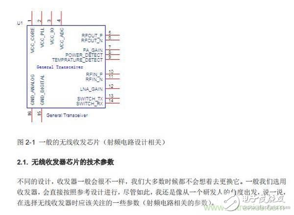
Figure 2-1 General wireless transceiver chip (related to RF circuit design)
2.1. Technical parameters of the wireless transceiver chip
Different designs, transceivers will generally be very different, we will not think about replacing it most of the time. Generally, we choose the transceiver, which will be directly in accordance with the reference design. However, I still talk about some parameters (RF circuit related parameters) that should be concerned when selecting a wireless transceiver from the perspective of a developer.
2.1.1. Protocol, frequency, path and transmission rate
In the transceiver's Datasheet, generally in the first few paragraphs, it is pointed out which protocols are supported by the chip, on what frequency, and several paths (that is, several shots). Our current main product design is Is supporting 802.11n. The importance of these three parameters must not be said by me, and everyone should understand it. Their parameters determine the function of the final product.
A typical description such as: The Atheros AR9220 is a highly integrated single-chip soluTIon for 2.4GHz and 5GHz 802.11n-ready wireless local area network (WLANs) that enables high-performance 2&TImes;2 MIMO configuraTIons for wireless staTIons applications demanding robust link Quality and maximum throughput and range.
From this description, we can know that the AR9220 supports the 802.11n draft (generally compatible with 802.11b/g). At the same time, the AR9220 also supports dual-band, 2.4GHz and 5GHz, so we can know that it also supports 802.11a. 2×2 MIMO Description The AR9220 is a second-in-two-out (2T2R).
Transmission rates are closely related to protocols and pathways, and interested colleagues can access relevant information.
From the AR9220's Datasheet, we can know that the 20MHz bandwidth, the maximum transmission rate can reach 130Mbps, the highest transmission rate can reach 300Mbps when the bandwidth is 40MHz.
2.1.2. Modulation method
The modulation mode and the transmission rate are closely related, and different transmission rates correspond to a different modulation mode. The modulation modes supported by the chip are generally given in the characterization of the Datasheet. For example, the AR9220 supports modulation methods such as BPSK, QPSK, 16QAM, 64QAM, DBPSK, DQPSK, and CCK.
2.1.3. Clock frequency
The clock frequency, the clock frequency includes two kinds, the frequency of the external crystal of the transceiver and the operating frequency after the internal multiplication. This parameter should also be our concern.
2.1.4. Output power
There is a phenomenon I have been confused about, why is it not given its transmit power in the transceiver's Datasheet? This parameter is very important for our RF engineers. Because this parameter determines the design of the subsequent power amplifier circuit, we must ensure that the output power of the transceiver is enough to drive the power amplifier, so that we can design a reasonable and effective amplifier.
2.1.5. Receive sensitivity
As with the output power, the transceiver receiving sensitivity parameter will not be given in the Datasheet. In the actual design process, with this parameter, we can reasonably design the amplification factor of the low noise amplifier to ensure low noise. The output of the amplifier can be effectively accepted by the transceiver.
2.1.6. RF interface
This parameter relates to the structure of our subsequent RF circuits. In general, the transceiver should have RF input pins including: RF output pin, power amplifier gain control pin, power amplifier output power detection input pin, low noise amplifier gain control pin, switch transceiver control pin In general, Ralink's solution will also have a PA temperature detection pin.
2.1.7. Supply voltage and power consumption
From a global perspective, the supply voltage and power consumption are also the technical parameters we have to pay attention to. These two parameters are related to the design of the power supply circuit and the design of the heat dissipation.
2.2. Processing of differential RF signals
2.2.1. The pins of the transceiver itself
For RF signals, in order to enhance the anti-interference ability of the transceiver, differential signal processing is generally adopted, that is, the transceiver transmits the signal in a differential form, and the external circuit must also provide a differential RF signal for the transceiver. enter. As shown in Figure 2-2, the four pins in the red box are the input of the differential RF signal of the transceiver, and the output pin is also the most important RF signal pin.
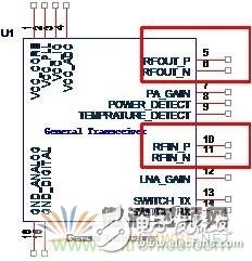
Figure 2-2 RF input and output pins of the transceiver
It must be pointed out here that Atheros' transceivers generally do differential processing of inputs and outputs at the same time. However, Ralink generally requires externally input signals to be differential, while the RF signals output by itself are not differential. Figure 2-3 and Figure 2-4 show the main RF signal pins for RT3052 (Ralink) and AR9220 (Atheros), respectively. It is not difficult to find that Atheros's design is more delicate than Ralink. It is not just a transceiver chip. In the design of subsequent circuits, Atheros will also consider the problems considered. I think this is what we should have as a developer. a spirit.
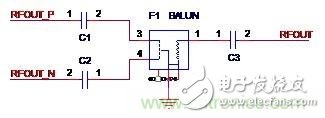
Figure 2-3 Main RF signal pins of the RT3052
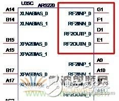
Figure 2-4 Main RF signal pins of the AR9220
2.2.2. Differential signals transmitted by the transceiver
The differential signals sent by the transceiver, we have to find a way to combine them into one. Why do you want to do this, the signal sent by the transceiver is to be given to the power amplifier circuit, and the power amplifier circuit is to process the single-ended signal.
Balancers are often used to deal with differential signal problems. In addition, we know that both inductors and capacitors can change the phase of the signal. From differential signals to single-ended signals, the basic method is to use inductors and capacitors to make two different In this way, the two signals passing through the processing circuit are 180° out of phase, so that the differential signals with the original phase difference of 180° can be in phase to obtain a single-ended signal. Conversely, a single-ended signal is passed through two different paths, resulting in a differential signal.
Let's take a look at the circuit form of the two methods separately.
Method one, use a balancer. The differential signal with a phase difference of 180° is passed through a balancer (Balun, commonly known as balun), and a single-ended RF signal can be obtained. As shown in Figure 2-5, F1 in the figure is a balancer. The differential signals RFOUT_P and RFOUT_N get the single-ended signal RF_OUT through F1.

Figure 2-5 Typical Balance Circuit
Method two, using discrete components. A typical processing circuit using discrete components is shown in Figure 2-6.
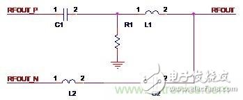
Figure 2-6 Typical discrete component processing circuit
2.2.3. Parameters and selection of the balancer
In Atheros's solution, the balancer is often used a lot, I will give the main parameters of the balancer and a brief selection guide. As mentioned earlier, in our Wi-Fi products, the balancer is often used to process differential signals. The main parameters are as follows:
Unbalanced impedance
Balanced impedance
working frequency
Unbalanced port return loss
Phase change
Insertion loss
For example, the typical parameters of the commonly used balancer HHM1711D1 are shown in Figure 2-7. In this way, we can choose the right balancer according to our needs.
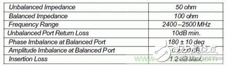
Figure 2-7 Typical parameters of the HHM1711D1
2.2.4. Differential signals received by the transceiver
The signal received by the transceiver comes from the low-noise amplifier at the front end. Like the power amplifier, the low-noise amplifier processes the single-ended RF signal, so we must convert the signal output from the low-noise amplifier. Similarly, there are two ways to handle the output signal of a low noise amplifier: using a balancer and using discrete components. Some of Atheros's solutions use balancers; Ralink's solution has not been used yet.
In fact, everyone must have thought that the transceiver receiving signal and the transceiver sending signal are almost the opposite process, so the structure of the circuit is almost the opposite. That's right, I saw the actual circuit diagram below. Let me introduce the scheme of using the balancer. In a practical case, the balancer circuit shown in Figure 2-8 is used. The single-ended signal RF_IN passes through the balancer F5 to obtain differential RF signals RFIN_P and RFIN_N.
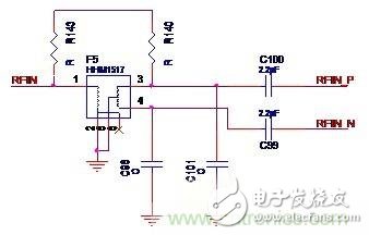
Figure 2-8 Balancer circuit used in a case
Let's take a look at the methods implemented with discrete components. Figure 2-9 shows the usual way of using Ralink. Figure 2-10 shows the common processing methods of Atheros. It can be seen that the two design methods are similar.
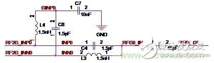
Figure 2-9 Ralink commonly used discrete component signal processing
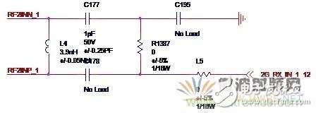
Figure 2-10 Atheros commonly used discrete component signal processing
2.3. Transceiver Power Pins
Transceivers generally have a large number of power pins, which can be roughly divided into several categories. As can be seen from Figure 2-2, there will be main power pins, core voltage power pins, IO power pins, phase-locked loops. (Phase Lock Loop, PLL) power pin, etc.
In the design of RF circuits, we generally pay more attention to analog power supplies. For the RF circuit power supply, if I choose between a linear regulated power supply (LDO) and a switching power supply (DC/DC), then I will not hesitate to choose a linear power supply.
why? And the switching power supply has hatred? There is indeed hatred!
Until now, I have clearly remembered the experience in the university. Once I designed a campus broadcasting equipment for a university, considering the large output power of campus broadcasting, the requirements for power supply were more demanding. I went to the technology market and found a well-made switching power supply. At that time, I was deceived by the gorgeous appearance of this guy and bought it without hesitation. However, when I was completely designed, I turned on the power, and the sound from the radio was not a pleasant music sound, but a very disgusting "squeaky" sound, a huge hum. In order to solve this problem, I almost racked my brains and redesigned the parts that might cause problems, but the problem remained unresolved. Later, I suddenly realized: "Is it a problem with switching power supplies?" Just have a car radio power supply (high-power linear regulated power supply). When I connect this power supply, wow, the whole world is quiet! Switching power supply not only lost some money, but also wasted a lot of time. Since then, my design has never used switching power.
For the power supply pins of the transceiver, the usual processing method is to place a 0.1uF capacitor at the pin of each power supply. Next to the power-consuming pins, a larger capacity capacitor, 1-10uF or Bigger. In general, the analog power supply and digital power supply of the transceiver should be separated by inductors or magnetic beads, and the capacitor with a relatively large capacity must be placed behind the inductor or the magnetic beads. If conditions permit, it is best to place the electrolytic capacitor. It will greatly improve the performance of the power supply. At the same time, several small-capacity ceramic capacitors can be connected in parallel to filter out the AC components of different frequencies.
2.4. Transceiver complete peripheral circuit design
Recall that in the previous description, we explained how to select the transceiver, the differential signal processing related to the transceiver, and the power supply of the transceiver. These three aspects basically cover the content of the transceiver RF circuit design. In other words, to understand these three parts, basically complete the design of this part.
Presumably everyone should be clear about the structure of the three parts, well, let us try, put some devices on the periphery of the chip in Figure 2-2, and then connect several lines to complete the wireless transceiver and its peripheral circuit design. Here, we process the differential signal output from the transceiver with a balancer to obtain a single-ended signal RFOUT. The received signal RFIN from the low-noise amplifier is processed by discrete components to obtain the differential signals RFIN_P, RFIN_N. In this way, the schematic shown in Figure 2-11 is obtained.
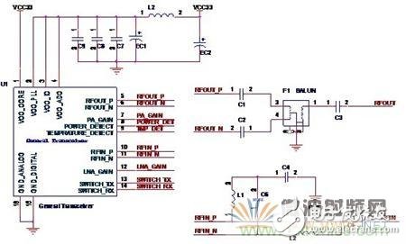
Figure 2-11 Completely designed wireless transceiver peripheral circuit
Chapter 3. Power Amplifiers
Power amplifier, Power Amplifier, commonly known as PA, is mainly used to power-amplify the RF signal sent by the radio transceiver (Radio Transceiver) to ensure that there is enough output power to meet the design requirements. The design of the power amplifier is a very professional topic, and there are many people. Many senior RF engineers have done in-depth research in this area. I will only discuss the common design methods of our Wi-Fi products here.
In our products, the composition of the power amplifier is nothing more than a chip with several peripheral devices, but in the case of high power, almost no one uses the integrated circuit for power amplification, which is generally designed with discrete components. , transistor or FET. In all of our current designs, power amplifiers are implemented using integrated circuits. As shown in Figure 3-1, it is a block diagram of the design of a typical power amplifier.
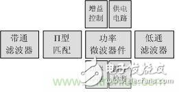
Figure 3-1 Block diagram of the power amplifier
The design of the power amplifier will consider many parameters, but it is mainly divided into three categories: gain, noise, and nonlinearity. The gain is related to the final output power, which is related to signal quality.
Here I will divide the power amplifier (referred to as the power amplifier in the following contents of this chapter) into the following sections: the selection of the power amplifier chip, the power supply of the power amplifier chip, the input loop, the output loop, the power detection, the gain control, and the temperature detection.
3.1.1. Pins of the power amplifier chip
The power amplifier chip belongs to the category of microwave power devices. Figure 3-2 shows the schematic symbol of a typical power amplifier chip, including the following pins:
VCC main power supply pin
VC1 primary power amplification power supply pin
VC2 secondary power amplification power supply pin
RFIN RF signal input pin
RFOUT RF signal output pin
One of the GAIN_1 gain control pins
GAIN_2 Gain Control Pin 2
POWER_DETECT built-in power detection output pin
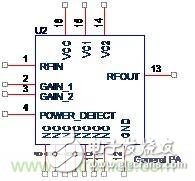
Figure 3-2 Typical power amplifier chip
It is worth noting that GAIN_1 and GAIN_2 are control signals from the Transceiver and are DC voltage. POWER_DETECT is the transmit power detection value of the output of the power amplifier chip, and is also the DC voltage. RFIN and RFOUT are the most important RF signal pins. .
3.1.2. Major manufacturers of power amplifier chips
Among the products on the market, the suppliers of power amplifier chips are basically these four: SiGe, SST, Microsemi, Richwave, Table 3-1, Table 3-2 shows the power amplifier chips used in several practical projects. model.
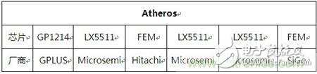
Table 3-1 Amplifier chips used in the design of Atheros
Table 3-2 Power amplifier chip used in Ralink design
From the above table, we can easily find out that Atheros likes Microsemi's chip, and Ralink prefers Richwave and SST. In the BCM4323 project, the power amplifier chip used is SiGe. In the current design of AP96, it is also used. SiGe's Frontend Module.
3.1.3. Main parameters of the power amplifier chip
The choice of power amplifier chip is a complicated process. In the actual selection process, we generally consider the following parameters:
working frequency
Small signal gain
Maximum linear output power
1dB compression point output power
Error vector magnitude (EVM)
Adjacent channel power ratio (ACPR)
Noise Figure
Whether built-in power detection function
Whether built-in gain control function
Supply voltage
Current consumed
The above parameters are not completely given in the Datasheet of each power amplifier chip, and some Datasheets can only give some parameters. The meaning of each parameter must be clear to everyone, I will not explain too much here. A typical power amplifier chip's Datasheet is as follows:
2.3-2.5GHz Operation
Single Positive Supply Voltage Vcc = 3.3V
Power Gain ~ 27dB
Quiescent Current ~ 90mA
EVM ~ -30dB at Pout = +19dBm
Total Current ~ 150mA for Pout = +19dBm
Pout ~ +26dBm for 11g OFDM Mask Compliance
Total Current ~220mA for Pout = +23dBm 1 Mbps DSSS
On-Chip Input Match
Simple Output Match
Robust RF Input Tolerance > +5dBm
Small & Low-Cost 3x3x0.9mm3 MLP Package
Cost Reduction over LX5510, LX5510B
From the above description, we learned that the power amplifier chip operates at 2.3-2.5 GHz and operates from a single 3.3V supply. The quiescent operating current is 90 mA. At 19 dBm power output, the EVM value is -30 dB.
The performance of the power amplifier chip is very important, of course, we will choose the cheapest when it meets the performance.
3.2. Power supply for the power amplifier chip
The general power amplifier chip shown in Figure 3-2 has three power pins, VCC, VC1, and VC2. VCC is the main power supply, VC1 is the first-stage amplified power supply inside the chip, and VC2 is the second-stage amplification inside the chip. Power supply. There is a very important issue here. VC1 and VC2 are not simple power supply pins. These two pins are usually not connected directly to the power supply. Usually, an inductor (or resistor) is connected in series and connected to the power supply. Why? What? This is because this is the pin that powers the power transistors (or FETs) inside the chip. Usually in a power amplifier circuit composed of separate components, we will see the collector at the transistor (or the drain of the FET). There are inductors on the strings, and the inductors are not easy to integrate into the chip. Therefore, it is necessary to place the inductor outside the chip. In this way, the power supply mode of the typical power amplifier chip is obtained, as shown in Figure 3-3.
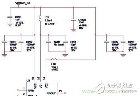
Figure 3-3 Typical power amplifier chip power supply mode
In addition to the above mentioned inductance problems, another important point is that the analog signal processed by the power amplifier circuit is a formal analog circuit, so it is necessary to pay special attention to the power supply to be separated from the power supply of the digital circuit. Another extremely important issue is that, as shown in Figure 3-3, a filter capacitor combination needs to be placed at each power pin. For example, a combination of 100pF and 1000pF filter capacitors is placed at the VCC pin. The foot is a 10pF capacitor. The combination of filter capacitors is such that for the main power supply pin VCC, it is necessary to place as many capacitors as possible, and the capacity of these capacitors is preferably of different order of magnitude, for example, it can be combined: 10uF+1uF+0.1uF+ 1000pF+100pF+10pF, different capacity capacitors are used to filter out the disturbance of different frequency components. For the two pins VC1 and VC2, it should be noted that the capacity of the filter capacitor placed is small, usually 1-10pF.
3.3. Input loop
The input circuit of the power amplifier circuit generally includes two parts, one is a Band Pass Filter (BPF), and the other is a åŒ¹é… type matching network. We are divided into two parts.
3.3.1. Bandpass filter
We know that there are 13 subcarriers in the 2.4 GHz band, the frequency is from 2.412 GHz to 2.437 GHz, and the frequency interval between adjacent channels is 500 MHz. It is easy to understand that the signal output from the transceiver (Transceiver) includes from 2.412. A frequency band from GHz to 2.437 GHz, therefore, in order to enable a useful signal to smoothly enter the power amplifier chip, useless messy signals are filtered out, and a band pass filter is generally placed on the input loop of the power amplifier chip.
There are three implementations of the bandpass filter. One is to use a dedicated bandpass filter that has been designed, which is used in many Ralink schemes; one is a bandpass filter composed of discrete components. Not a lot; the third method is almost proprietary to Atheros, which is a printed bandpass filter. The most prominent advantage of this filter is that it has no cost. The most prominent shortcoming is that it takes up a lot of space and requires clearance. Zone, this filter is used in AP51.
Designing a bandpass filter with discrete components requires a complicated calculation process and requires a strong mathematical foundation. We do not do much research here. Next we will discuss how to choose a bandpass filter that has been designed. There are not many parameters of the bandpass filter, mainly:
input resistance
Output impedance
Passband
Attenuation in the passband
Attenuation outside the passband
Normally, the finished bandpass filter, the input and output impedances are controlled to a nominal value of 50 ohms, and a chart is sufficient to reflect the characteristics of the passband. Figure 3-4 shows the relationship between the S21 parameters and frequency of our commonly used HMD845H. It is obvious that the pass band of the band pass filter is 2.4 GHz to 2.5 GHz, and the fading is fast for frequencies outside the pass band.
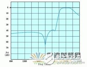
Figure 3-4 S21 parameters of the HMD845H
3.3.2. Type matching network
Matching, this matter is extremely important in RF design. Many times, we design or debug RF circuits, all of which are solving the matching problem. Always remember such a classic criterion: conjugate matching transmission power is the largest. The 匹é…-type matching network is usually placed directly at the input end of the power amplifier chip, that is, at the pin of RFIN. Usually, the pin of the chip will not match 50 ohms, and we will not know the input characteristics of the pin. In this case, The need for a 匹é…-type matching network can be imagined.
The 匹é…-type matching network, as the name implies, looks like a letter Î , let's take a look at the actual 匹é…-type matching network. Figure 3-5 shows a type of matching network commonly used by Ralink.
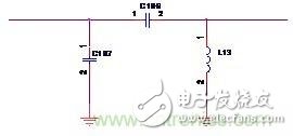
Figure 3-5 Ralink commonly used type matching network
3.3.3. Completely designed input loop
Above we discussed the two components of the input loop of the power amplifier circuit, the bandpass filter and the 匹é…-type matching network. With these two parts, we can design a complete input loop. As shown in Figure 3-6, it is a complete design of the input circuit of the power amplifier circuit. The U9 in the figure is a finished bandpass filter, while the C108, C109 and L14 form a 匹é…-type matching network.
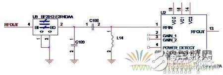
Figure 3-6 Input circuit of a fully designed power amplifier circuit
3.4. Output loop
In the output loop, the most important component (and the only component in many designs) is the low-pass filter. At this point, someone might ask why the low-pass filter is used here instead of the input loop. Bandpass filter? The reason is very simple. The main problem to be solved by the low-pass filter here is due to the higher harmonics caused by the power amplifier, such as the second harmonic, the third harmonic or even higher harmonics. Of course, the low-pass filter still needs to be The problem solved is the matching problem. In fact, in the design of RF circuits, this problem of matching will always be with us.
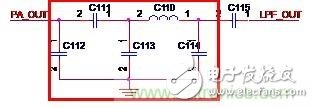
The design of the filter requires very complicated calculations. I don't want to explore too much theoretical knowledge here, so I don't give a way to calculate it, just give the general form of low-pass filter. It should be noted here that Atheros's design generally uses three components, while Ralink generally uses five components. As shown in Figure 3-7, it is a commonly used filter form of Ralink. In the figure, C112, C111, C113, C110 and C114 form a low-pass filter, and the signal PA_OUT from the power amplifier chip passes through the filter to obtain the LPF_OUT signal and sends it to the subsequent circuit.
At this time, we can connect the output of the power amplifier chip to the low-pass filter, and get the complete output loop of the general RF power amplifier circuit, as shown in Figure 3-8.
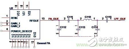
Figure 3-8 Completely designed power amplifier output loop
3.5. Power detection
The power detection function can be found in many of our designs. This function allows the radio transceiver (Radio Transceiver) to monitor the output power of the amplifier circuit at all times, so that when the output power of the amplifier changes, the wireless transceiver can be adjusted. The output power of the amplifier or the gain of the power amplifier circuit stabilizes the output power of the power amplifier circuit at a fixed value.
The power detection circuit outputs a DC voltage value. After the voltage value is sent to the wireless transceiver, the wireless transceiver itself performs A/D conversion, and the output power of the power amplifier circuit can be known.
There are usually two methods for power detection. In the design of Ralink, the power detection function of the power amplifier chip is usually used. In the design of Atheros, in addition to the power detection function of the power amplifier chip itself, there is usually one Atheros. The unique design we will discuss in two parts.
3.5.1. On-chip power detection
As we have seen in Figure 3-2, the general power amplifier chip has a pin such as POWER_DETECT, which is used for power detection. The chip's built-in power detection feature simplifies circuit design, as shown in Figure 3-9.
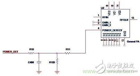
Figure 3-9 Common circuit forms using built-in power detection
3.5.2. Power detection circuit on the periphery of the chip
Here we use a separate section to discuss the peripheral detection circuit. In fact, it is Atheros's solution, because this design is too personal, let us see it together. As shown in Figure 3-10, it is the power detection scheme commonly used by Atheros. The PC1 in the figure is a Printed Coupler. The output signal LPF_OUT from the power amplifier passes through the coupler, and the high-frequency alternating voltage is sensed at pins 2 and 3. This voltage increases with the output power. Increase L18, L19, D1, C217, R248 to form a conventional rectifier circuit, so that the DC voltage POWER_DETECT changes with the change of output power, the wireless transceiver can get this voltage value and make corresponding action.
One thing to note here is that the rectifier diode D1 must select a diode with a high operating frequency. For example, the SMS7630 in this design operates at 10 GHz.
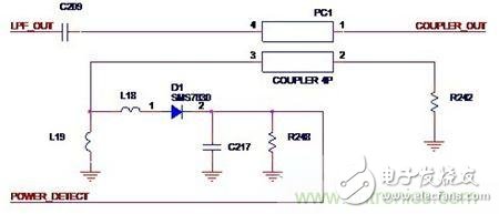
Figure 3-10 Power detection scheme commonly used by Atheros
3.6. Gain control
The function of the gain control is to change the gain of the power amplifier circuit so that the output power can be changed. There are two ways to change the final output power of a power amplifier. One is to change the output power of the wireless transceiver, and the other is to change the gain of the power amplifier circuit. Here we mainly focus on the latter. Usually, there are two or more gain control pins of the power amplifier chip, which change the gain values ​​of the first stage amplification and the second stage amplification respectively. Figure 3-11 is a typical gain control principle diagram. The control signal PA_GAIN from the transceiver is controlled by the RC filter circuit consisting of R245 and C248 (filtering out the possible AC component from the transceiver) by two resistors acting on the two pins GAIN_1 and GAIN_2 of the power amplifier chip, thereby controlling the power amplifier circuit. The gain also controls the final output power.
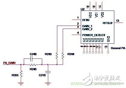
Figure 3-11 Typical gain control schematic
3.7. Temperature detection
The temperature detection function is used in many of Ralink's solutions, but it has not been seen in Atheros's solution. This function can detect the temperature of the power amplifier chip and prevent the chip temperature from overheating and burning. Another more important role is to adjust the output power of the power amplifier circuit according to the ambient temperature. In many cases, the change in ambient temperature will have a relatively large impact on the output power of the power amplifier chip. If the wireless transceiver knows the current temperature through the temperature detection circuit and adjusts its output power or changes the gain of the power amplifier properly, It is possible to maintain a stable power output of the power amplifier circuit when the ambient temperature changes, which is beneficial for improving the stability of the product.
Figure 3-12 shows a typical temperature sensing circuit for Ralink. RT1 in the figure is a thermistor. When the ambient temperature changes, its resistance changes. So, it is obvious that the value of TMP_DET will change, so that the transceiver can detect the temperature of the environment. The temperature sensing circuit is typically placed near the power amplifier chip.
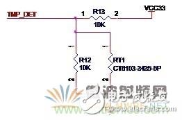
Figure 3-12 Ralink commonly used temperature detection circuit
3.8. Completely designed power amplifier circuit
In the above, we discussed the various components of the power amplifier circuit. Now, let's combine these parts together to complete the design of the power amplifier circuit, as shown in Figure 3-13. Let's take a look, try to find out the previous parts, if you can, then you have a basic understanding of the general power amplifier circuit architecture of Wi-Fi products.
Usually, a reference design will be given in the data sheet of the power amplifier chip, which has a certain guiding effect on our design.
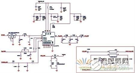
Figure 3-13 Completely designed RF power amplifier circuit
Chapter 4. Low Noise Amplifier
低噪声放大器在框图1-1ä¸ä½äºŽæ”¶å‘切æ¢å™¨ï¼ˆTransmit/Receive Switchï¼‰å’Œæ— çº¿æ”¶å‘器(Radio Transceiver)之间,对天线感应到的信å·è¿›è¡Œæ”¾å¤§ï¼Œè¿™æ ·æ‰èƒ½ä½¿æ— 线收å‘器进行有效的处ç†ã€‚å¯ä»¥è¯´ï¼Œä½Žå™ªå£°æ”¾å¤§å™¨çš„性能直接影å“ç€æ•´ä¸ªè®¾è®¡çš„çµæ•åº¦ã€‚
低噪声放大器的框图如图4-1所示,有四个部分组æˆï¼Œè¾“入回路,输出回路,放大电路,增益控制,在以下的内容ä¸ï¼Œæˆ‘们将é€ä¸ªè®¨è®ºã€‚
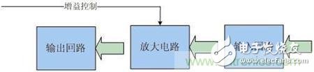
图4-1 低噪声放大器的框图
4.1. 低噪声的放大器的主è¦å‚æ•°
低噪声放大器,顾åæ€ä¹‰ï¼Œå°±å¯ä»¥çŸ¥é“其具有æžä½Žçš„噪声系数。噪声系数的物ç†å«ä¹‰æ˜¯ï¼šä¿¡å·é€šè¿‡æ”¾å¤§å™¨ä¹‹åŽï¼Œç”±äºŽæ”¾å¤§å™¨äº§ç”Ÿå™ªå£°ï¼Œä½¿ä¿¡å™ªæ¯”å˜å;信噪比下é™çš„å€æ•°å°±æ˜¯å™ªå£°ç³»æ•°ã€‚
é™¤äº†å™ªå£°ç³»æ•°ä»¥å¤–ï¼Œä»¥ä¸‹å‡ ä¸ªå‚数也是我们需è¦å…³æ³¨çš„:
功率增益
增益平å¦åº¦
工作频带
动æ€èŒƒå›´
功率增益主è¦å°±æŒ‡ä½Žå™ªå£°æ”¾å¤§å™¨çš„增益能力,增益平å¦åº¦æ述放大器在工作频带内频率å˜åŒ–引起的功率增益的波动,工作频带就是指放大器的æ£å¸¸å·¥ä½œçš„频率范围,动æ€èŒƒå›´æ˜¯æŒ‡æ”¾å¤§å™¨å…许输入的最å°å’Œæœ€å¤§åŠŸçŽ‡èŒƒå›´ã€‚
4.2. 低噪声微波器件的选择
芯片或者晶体管(场效应管)的选择,以下简称微波器件的选择,往往对于低噪声放大器的设计起ç€è‡³å…³é‡è¦çš„å½±å“。我们先æ¥çœ‹ä¸€çœ‹åœ¨æˆ‘们公å¸çš„设计ä¸ï¼Œé€šå¸¸é€‰ç”¨ä»€ä¹ˆå¾®æ³¢å™¨ä»¶ã€‚表4-1和表4-2给出了Atheroså’ŒRalink常用的低噪声放大器微波器件。
我们ä¸éš¾å‘现,这些器件的选择没有太多的共性,我们能看到有四ç§è§£å†³æ–¹æ¡ˆï¼Œç¬¬ä¸€ç§æ˜¯é‡‡ç”¨å¾®æ³¢ä¸‰æžç®¡æ¥å®žçŽ°ï¼Œç¬¬äºŒç§æ˜¯ä½¿ç”¨ä¸“用低噪声放大器芯片,第三ç§æ˜¯é›†æˆåœ¨å‰ç«¯æ¨¡å—(Frontend Module)ä¸ï¼Œç¬¬å››ç§å°±æ˜¯ä¸ä½¿ç”¨ä½Žå™ªå£°æ”¾å¤§å™¨ã€‚我们在这里åªè®¨è®ºé‡‡ç”¨æ™¶ä½“管和专用芯片的方法。
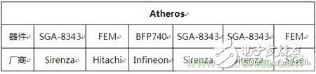
表4-1 Atheros常用的低噪声放大器微波器件
微波器件(晶体管或芯片)的å‚数,基本上就决定了低噪声放大器的性能,我们æ¥çœ‹ä¸€ä¸‹æœ€å¸¸ç”¨çš„SGA-8343çš„å‚数,如图4-2所示。图ä¸ç»™å‡ºçš„å‚数包括最大增益,噪声系数,S21,工作频率,供电电压,消耗的电æµç‰ç‰ã€‚对于专用的低噪声放大器芯片,å‚数也基本如æ¤ï¼Œåœ¨è¿™é‡Œæˆ‘们就ä¸è¯¦ç»†è¯´äº†ã€‚
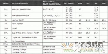
图4-2 SGA-8343çš„å‚数表
4.3. 输入回路
å’ŒåŠŸçŽ‡æ”¾å¤§å™¨ä¸€æ ·ï¼Œä½Žå™ªå£°æ”¾å¤§å™¨çš„è¾“å…¥å›žè·¯ä¸ä¹Ÿä¼šæœ‰åŒ¹é…网络,但是Atheros好åƒæ˜¯ä¸èµ°å¯»å¸¸è·¯ï¼Œå¾ˆå°‘看到低噪放的输入匹é…网络,而Ralink则ä¸ä¸€æ ·ï¼Œå‡ 乎在æ¯ä¸ªè®¾è®¡ä¸éƒ½ä¸è§„ä¸çŸ©çš„使用Π型匹é…网络,如图4-3所示,就是Ralink常用的Π型匹é…网络,我个人是比较推崇这ç§åšæ³•çš„。有了匹é…网络,我们å¯ä»¥æœ€å¤§é™åº¦çš„ä¿è¯æˆ‘们的设计是高性能的,也就是High-Performance。
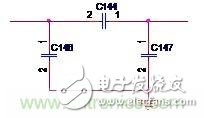
图4-3 Ralink常用的Π型匹é…网络
4.4. 输出回路
å’Œè¾“å…¥å›žè·¯ä¸€æ ·ï¼Œè¾“å‡ºå›žè·¯é€šå¸¸ä¹Ÿä¼šæ”¾ç½®åŒ¹é…网络,åŒæ ·ï¼ŒAtheros一般还是ä¸è¿™æ ·åšï¼Œä»–们最多会放置一个专有的å°åˆ¶å¸¦é€šæ»¤æ³¢å™¨ï¼ˆPrinted Band Pass Filter),Ralink的输出回路上的Π型匹é…网络基本上会输入回路上的一致,在这里ä¸ç»™å‡ºå…·ä½“çš„å½¢å¼äº†ã€‚
4.5. 电æºä¸Žå¢žç›ŠæŽ§åˆ¶
增益控制的作用是很明显的,当接收到的信å·å¼ºåº¦è¾ƒä½Žæ—¶ï¼Œæˆ‘们å¯ä»¥æ高低噪声放大器的增益,ä¿è¯ä¿¡å·å¯ä»¥æ£å¸¸è¢«æŽ¥æ”¶ï¼›å½“接收信å·çš„强度较高时,å¯ä»¥é™ä½Žä½Žå™ªå£°æ”¾å¤§å™¨çš„增益,以å…é€ æˆä¿¡å·é˜»å¡žã€‚这就是所谓的自动增益控制(Auto Gain Control,AGC)åŒæ ·ï¼Œè¿™å¯¹äºŽæ高产å“的稳定性,是很é‡è¦çš„。
我为什么è¦æŠŠç”µæºä¸Žå¢žç›ŠæŽ§åˆ¶æ”¾åœ¨åŒä¸€èŠ‚å‘¢ï¼Ÿå› ä¸ºä½Žå™ªå£°æ”¾å¤§å™¨çš„å¢žç›Šæ˜¯ä¾é 改å˜ä¾›ç”µç”µåŽ‹æ¥å®žçŽ°çš„ï¼Œè¿™æ ·å°±å¾ˆå®¹æ˜“ç†è§£äº†ã€‚å¦è¿‡æ¨¡æ‹Ÿç”µè·¯çš„都会知é“,三æžç®¡æ”¾å¤§ç”µè·¯çš„放大å€æ•°å’Œä¾›ç”µç”µåŽ‹æœ‰å¯†åˆ‡å…³ç³»ï¼Œå¯¹äºŽèŠ¯ç‰‡è¯´ä¹ŸåŒæ ·å¦‚æ¤ã€‚图4-4给出了常è§çš„增益控制的电路形å¼ã€‚图ä¸çš„LNA_GAIN既是æ¥è‡ªæ— 线收å‘器(Radio Transceiver)增益控制信å·ï¼Œåˆæ˜¯ä½Žå™ªå£°æ”¾å¤§å™¨çš„供电电æºï¼ŒC104是滤波电容,显而易è§ï¼Œä½Žå™ªå£°æ”¾å¤§å™¨çš„增益直接与LNA_GAIN的电压有关。
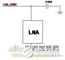
图4-4 常è§çš„增益控制的电路形å¼
4.6. 完整设计的低噪声放大器
在这里,我è¦å‘大家展示的是一款设计å分细腻的低噪声放大器,这也是我è§è¿‡çš„设计最为优秀的低噪声放大器,就是æ¥è‡ªæŸå®žé™…案例ä¸çš„2.4GHz频段的放大器,让我们æ¥ä¸€åŒé¢†ç•¥å®ƒçš„风采,如图4-5所示。
图ä¸çš„LNA_GAIN是æ¥è‡ªæ— 线收å‘器(Radio Transceiver)的增益控制信å·ï¼Œæ”¾å¤§å™¨ä½¿ç”¨çš„晶体管就是最常用的SGA-8343,R238,R239,R240是基æžçš„å置电阻,C219,L20,C220组æˆäº†ä½Žé€šæ»¤æ³¢å™¨ï¼Œæ¥è‡ªåˆ‡æ¢èŠ¯ç‰‡ï¼ˆSwitch)的LNA_IN通过低通滤波器之åŽç»ç”±C218耦åˆè‡³ä½Žå™ªå£°æ”¾å¤§å™¨ï¼ŒQ2与C221,L51,C214,R240,C210,R239,R238,C211,R241,C215,L52组æˆäº†å…±å°„æžæ”¾å¤§ç”µè·¯ï¼Œæœ€ç»ˆè¾“出RFINé€è‡³æ”¶å‘器进行处ç†ã€‚
尤其值得我们注æ„的是,在æ¯ä¸€ä¸ªèŠ‚ç‚¹å¤„ï¼Œéƒ½æ”¾ç½®äº†æ»¤æ³¢ç”µå®¹ï¼Œè¿™æ ·ï¼Œå°±å¯ä»¥æœ€å¤§é™åº¦çš„消除任何å¯èƒ½çš„噪声,从而实现性能优秀的低噪声放大电路。
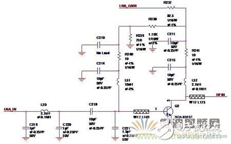
图4-5 æŸå®žé™…案例ä¸è®¾è®¡ç²¾è‰¯çš„低噪声放大器
第5ç« . 收å‘切æ¢ç”µè·¯
收å‘切æ¢ç”µè·¯å®žçŽ°çš„功能就是进行å‘射与接收的切æ¢ï¼Œé€šå¸¸å…¶æœ€é‡è¦çš„组æˆéƒ¨åˆ†å°±æ˜¯ä¸€é¢—芯片,我们分æˆå››ä¸ªéƒ¨åˆ†æ¥è®¨è®ºï¼šèŠ¯ç‰‡çš„选择,å‘射与接收回路,天线回路,控制管脚的处ç†ã€‚
5.1. 切æ¢èŠ¯ç‰‡çš„选择
切æ¢èŠ¯ç‰‡åœ¨ç»“构上,通常就是一个å•åˆ€åŒæŽ·çš„开关,开关掷å‘å“ªä¸€è¾¹å†³å®šäºŽåŠ åœ¨æŽ§åˆ¶ç®¡è„šä¸Šçš„ç”µåŽ‹ã€‚åˆ‡æ¢èŠ¯ç‰‡çš„典型内部结构如图5-1所示。
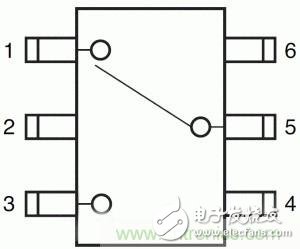
图5-1 切æ¢èŠ¯ç‰‡å…¸åž‹çš„内部结构
在选择切æ¢èŠ¯ç‰‡æ—¶ï¼Œæˆ‘们主è¦å…³æ³¨ä»¥ä¸‹å‡ 个å‚数:
working frequency
切æ¢é€Ÿåº¦
å…³æ–的隔离度
导通的衰å‡
能够承å—的功率
控制电压
功率消耗
有一个比较奇怪的现象时我们很少看到在Datasheetä¸æ到切æ¢é€Ÿåº¦è¿™æ ·çš„å‚数。在ç»å¤§å¤šæ•°è®¾è®¡ä¸ï¼Œå‡ ä¹Žæ— ä¸€ä¾‹å¤–çš„ä½¿ç”¨äº†NECå…¬å¸çš„uPG2179作为切æ¢èŠ¯ç‰‡ï¼ˆSwitch),其典型å‚数如图5-2 所示。
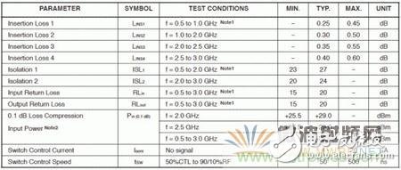
图5-2 切æ¢èŠ¯ç‰‡çš„典型å‚æ•°
5.2. å‘射与接收回路
切æ¢èŠ¯ç‰‡ä½äºŽé 近天线的地方,决定ç€å¤©çº¿ä½œä¸ºå‘射天线还是作为接收天线。功率放大器和低噪声放大器都会直接与切æ¢èŠ¯ç‰‡ç›¸è¿žï¼Œè¿™æ ·ï¼Œå‘射与接收回路上的匹é…就是必ä¸å¯å°‘的。关注一下Atheroså’ŒRalink的方案,会å‘现,Atheros会在å‘射回路上放置Π型匹é…网络,但是Ralink则ä¸ä¼šï¼Œä¸€èˆ¬å°±æ˜¯é€šè¿‡ç”µå®¹ç›´æŽ¥è€¦åˆã€‚
如图5-3所示,就是Atheros的典型å‘射与接收回路SW10就是那颗切æ¢èŠ¯ç‰‡ã€‚LPF_OUT是æ¥è‡ªåŠŸçŽ‡æ”¾å¤§å™¨çš„输出信å·ï¼ŒR186,C121与R194组æˆäº†Î 型匹é…网络,LNA_IN是é€è‡³ä½Žå™ªå£°æ”¾å¤§å™¨çš„ä¿¡å·ï¼ŒSWITCH_TX与SWICTH_RX这两个信å·çš„组åˆå°±æŽ§åˆ¶ç€æ˜¯æ‰“å¼€å‘射通路还是打开接收通路。
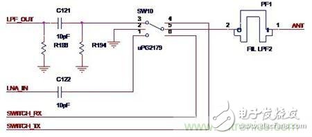
图5-3 Atheros的典型的å‘射与接收回路
5.3. 天线回路
在5-4ä¸æˆ‘们已ç»çœ‹åˆ°ï¼Œåœ¨Atheros的方案ä¸ï¼Œä¼šåœ¨å¤©çº¿å›žè·¯ä¸æ”¾ç½®ä¸€ä¸ªå°åˆ¶æ»¤æ³¢å™¨ï¼ˆPrinted Filter),图ä¸çš„PF1就是Atheros专有的å°åˆ¶æ»¤æ³¢å™¨ã€‚åŒæ ·ï¼ŒRalink一般也ä¸ä¼šåœ¨å¤©çº¿å›žè·¯ä¸è®¾ç½®æ»¤æ³¢å™¨æˆ–匹é…电路。
5.4. 控制信å·çš„处ç†
我们已ç»çŸ¥é“,图5-4ä¸çš„SWITCH_TXå’ŒSWITCH_RX是æ¥è‡ªæ— 线收å‘器(Radio Transceiver)的控制信å·ï¼Œæ˜¯ç›´æµç”µåŽ‹ï¼Œè¿™æ ·ï¼Œä¸ºäº†ç¨³å®šè¿™ä¸ªç”µåŽ‹å€¼ï¼Œé¿å…é€ æˆåˆ‡æ¢å™¨çš„误动作,我们一般会在控制通路上串è”一个电阻(或电感),一般是å°äºŽ1K的电阻,并且在控制管脚的ä½ç½®æ”¾ç½®æ»¤æ³¢ç”µå®¹ï¼ˆ1-10pFï¼‰ï¼Œè¿™æ ·ï¼Œæˆ‘ä»¬å°±å¯ä»¥å¾ˆå¥½çš„ä¿è¯åˆ‡æ¢èŠ¯ç‰‡æ²¡æœ‰è¯¯åŠ¨ä½œï¼Œä»Žè€Œï¼Œæˆ‘们就得到了如图5-4所示的完整的切æ¢ç”µè·¯çš„设计。
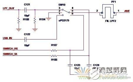
图5-4 完整设计的切æ¢ç”µè·¯
第6ç« . 天线与天线连接器
åœ¨è¿™ä¸€ç« é‡Œï¼Œæˆ‘è¦è®²çš„ä¸æ˜¯å¤©çº¿çš„è®¾è®¡ï¼Œå› ä¸ºç›®å‰æˆ‘还ä¸å¤ªæ‡‚天线设计,而且天线设计是一个å分专业和å¤æ‚çš„å¦ç§‘。在这里我想è¦è¯´çš„其实就åªæ˜¯ä¸€ä¸ªé—®é¢˜ï¼šä¸€å®šè¦åœ¨å¤©çº¿æˆ–者天线连接器的附近放置一个Π型匹é…网络,这一点是我们åšå°„频设计的人必须è¦ç‰¢è®°çš„事实。看一下Atheros å’ŒRalink的方案,会å‘现Π型匹é…网络是必ä¸å¯å°‘的,典型的设计如图6-1所示。
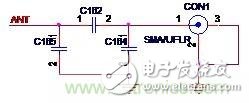
图6-1 典型的天线连接器电路设计
第7ç« . 完整设计的射频电路
在å‰é¢å‡ ç« çš„å†…å®¹ä¸ï¼Œæˆ‘们分æˆäº”ç« åˆ†åˆ«è®²è§£äº†å°„é¢‘ç”µè·¯çš„æ— çº¿æ”¶å‘器(Radio Transceiver),功率放大电路(Power Amplifier,PA),低噪声放大器(Low Noise Amplifier,LNA),收å‘切æ¢ç”µè·¯ï¼ˆTransmit/Receive Switch),天线与天线连接器(Antenna And Connector),在æ¯ç« 的最åŽä¸€èŠ‚,我们都给出了æ¯ä¸€éƒ¨åˆ†çš„å®Œæ•´è®¾è®¡ã€‚æˆ‘æƒ³ä½ å·²ç»çŸ¥é“了——没错,åªè¦æŠŠæˆ‘们æ¯ä¸ªéƒ¨åˆ†çš„完整设计组åˆåœ¨ä¸€èµ·ï¼Œé‚£ä¹ˆæˆ‘们就得到了Wi-Fi产å“的一般射频电路的完整设计,我们ä¸è¦æ€¥ï¼Œæˆ‘们å†æ¥å›žé¡¾ä¸€ä¸‹åœ¨æœ¬æ–‡ä¸€å¼€å§‹æ到的射频设计框图,如图7-1。相信大家这时一定已ç»å¯ä»¥æŠŠæ¯ä¸€ä¸ªéƒ¨åˆ†ç»†åŒ–ï¼Œå¾—åˆ°æ›´åŠ è¯¦ç»†çš„å°„é¢‘è®¾è®¡æ¡†å›¾ã€‚
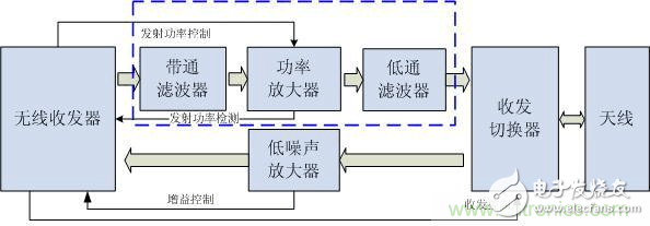
图7-1 射频设计框图
通过å‰é¢çš„讨论,我们已ç»çŸ¥é“,功率放大器是由带通滤波器,Π型匹é…网络,功率微波器件,增益控制,供电电路,功率检测,温度检测低通滤波器这些部分组æˆçš„;低噪声放大器是由Π型匹é…网络,低噪声放大电路和增益控制组æˆçš„;收å‘切æ¢å™¨æ˜¯ç”±Î 型匹é…网络,切æ¢èŠ¯ç‰‡ï¼Œæ»¤æ³¢å™¨ç»„æˆçš„;天线和连线连接器部分是由Π型匹é…网络和连接器组æˆçš„。于是,我们得到了Wi-Fi产å“一般射频电路的详细框图,如图7-2所示。
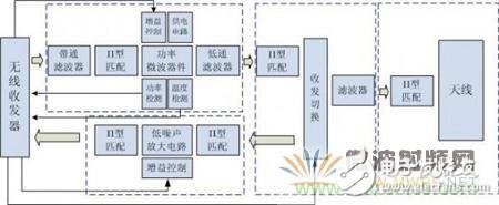
图7-2 射频设计详细框图
现在,让我们将å„个模å—的详细电路图,看看我们得到了什么。没错,我们得到了完整的设计图,如图7-3所示。在这个原ç†å›¾ä¸ï¼Œæˆ‘们设计的是一收一å‘的情况,如果是二å‘二收,那么原ç†å›¾å°±æ˜¯ä¸¤ä¸ªå›¾7-3,å¤åˆ¶è€Œå·²ã€‚
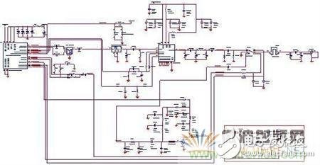
图7-3 完整详细的原ç†å›¾
由于时间有é™ï¼Œç¼–å†™è€…æ°´å¹³æ›´åŠ æœ‰é™ï¼Œé”™è¯¯ä¹‹å¤„在所难å…,欢迎大家批评指æ£ã€‚
We cover many types of Connectors for industrial, electrical and automotive, such as IP68 and waterproof connectors, OBD diagnostic connectors, also the standard or custom-designed power connectors for MINI FIT, MICRO FIT, MATE-N-LOCK.
Connectors System,Board System Connector,Efi System Injector Connector,Efi System Car Connector
ETOP WIREHARNESS LIMITED , http://www.wireharness-assembling.com